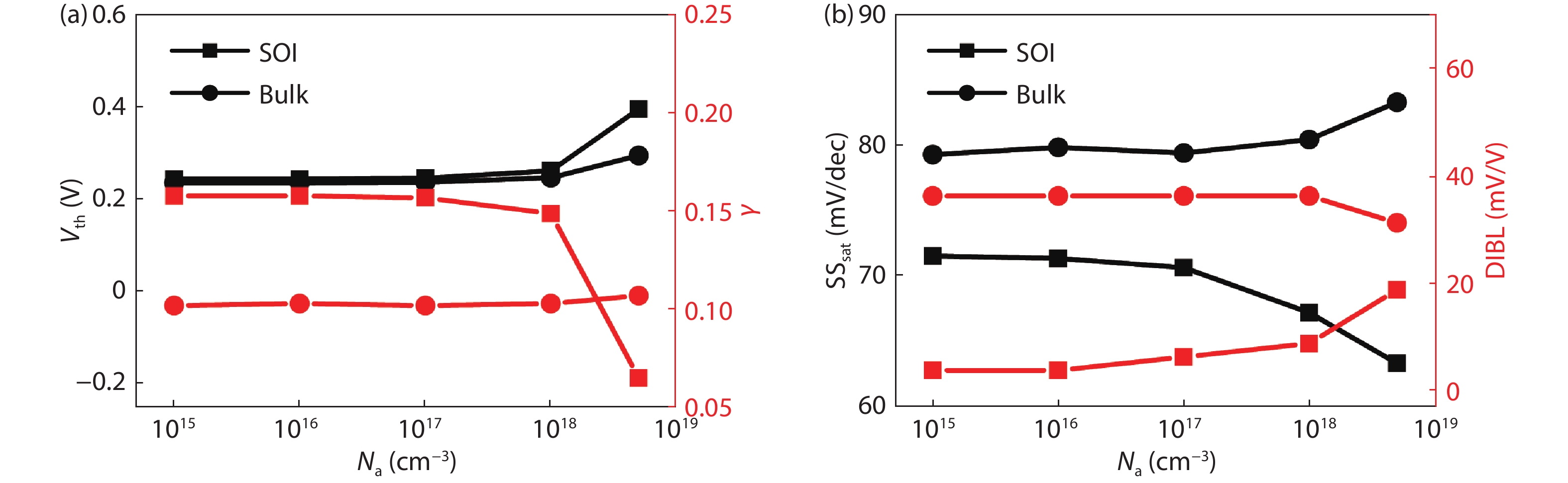
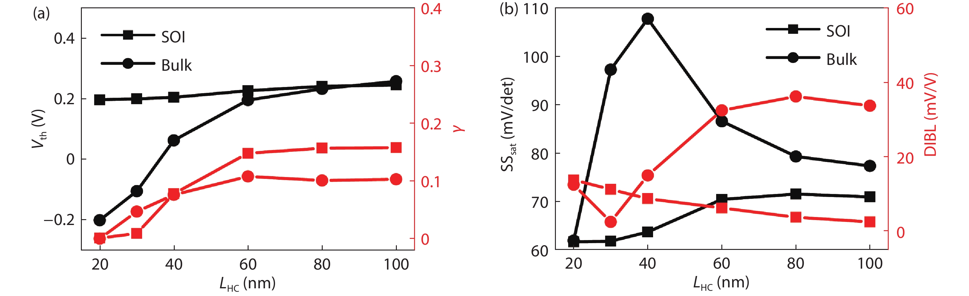
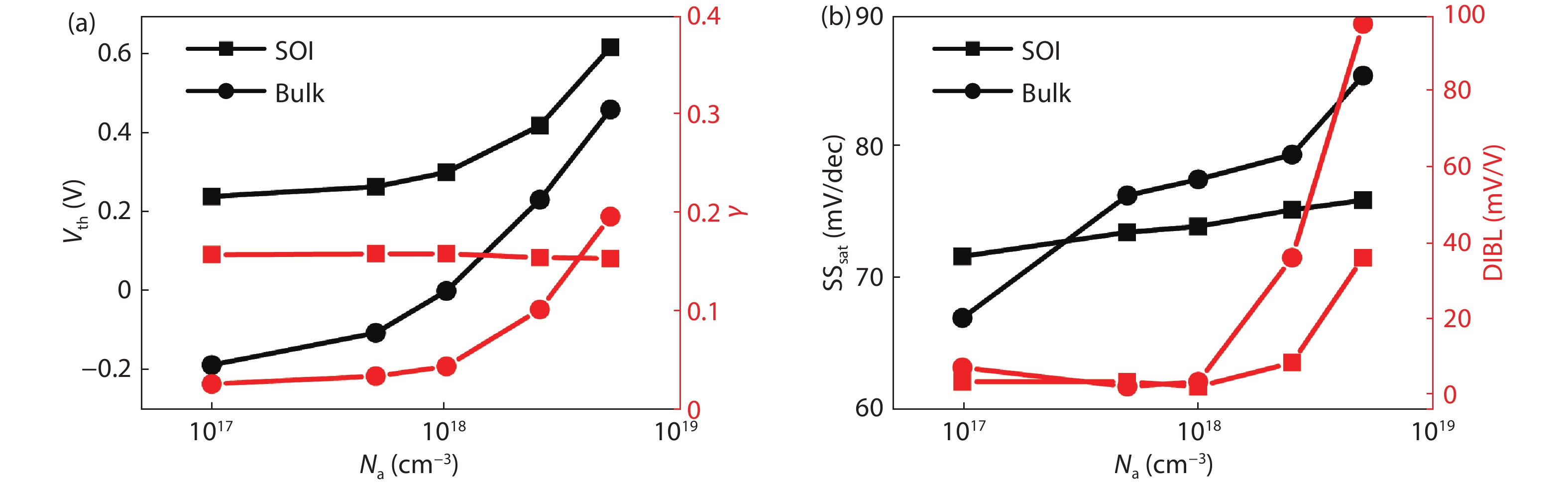
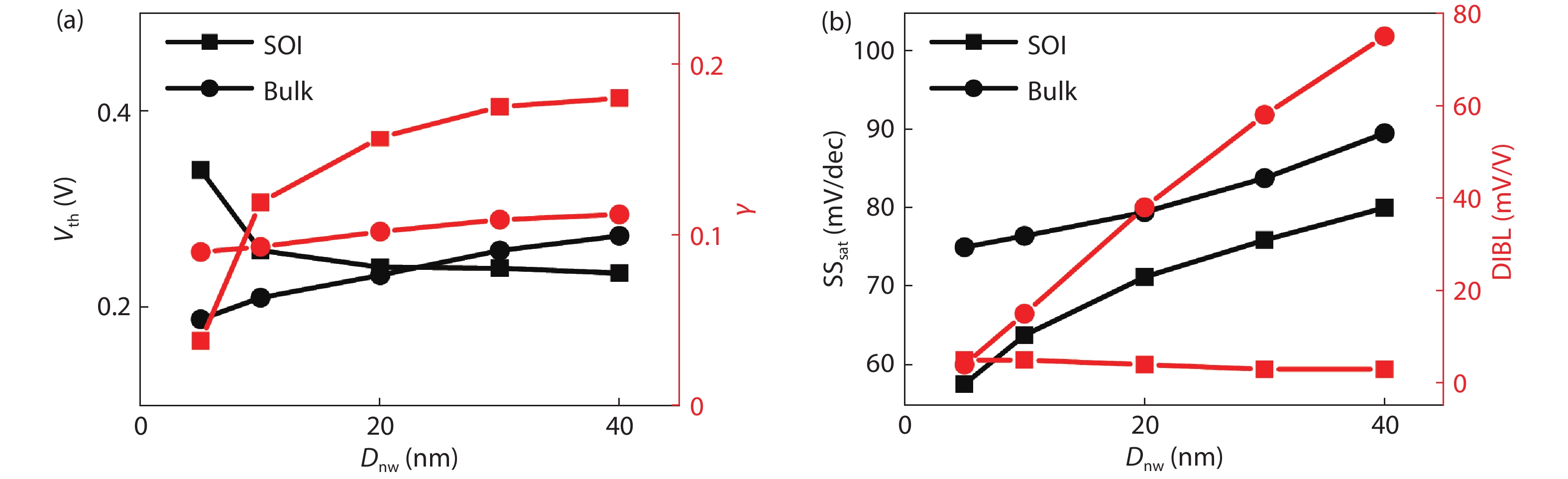
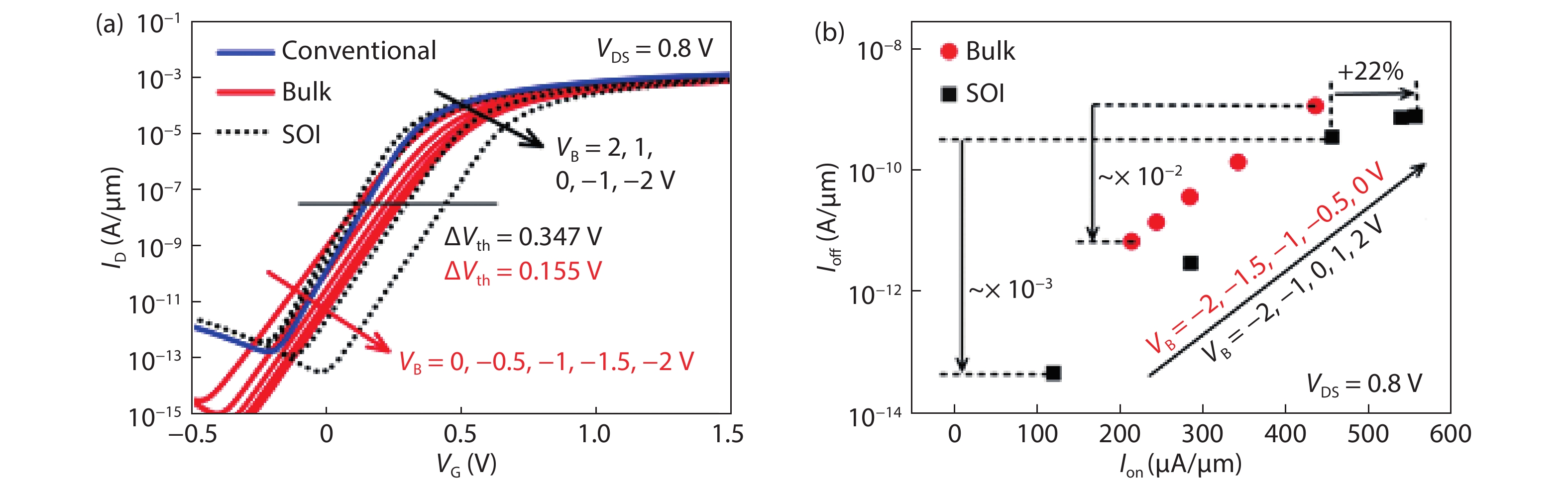
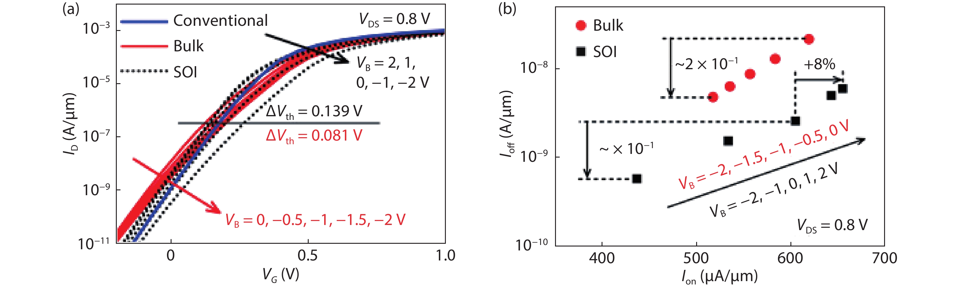
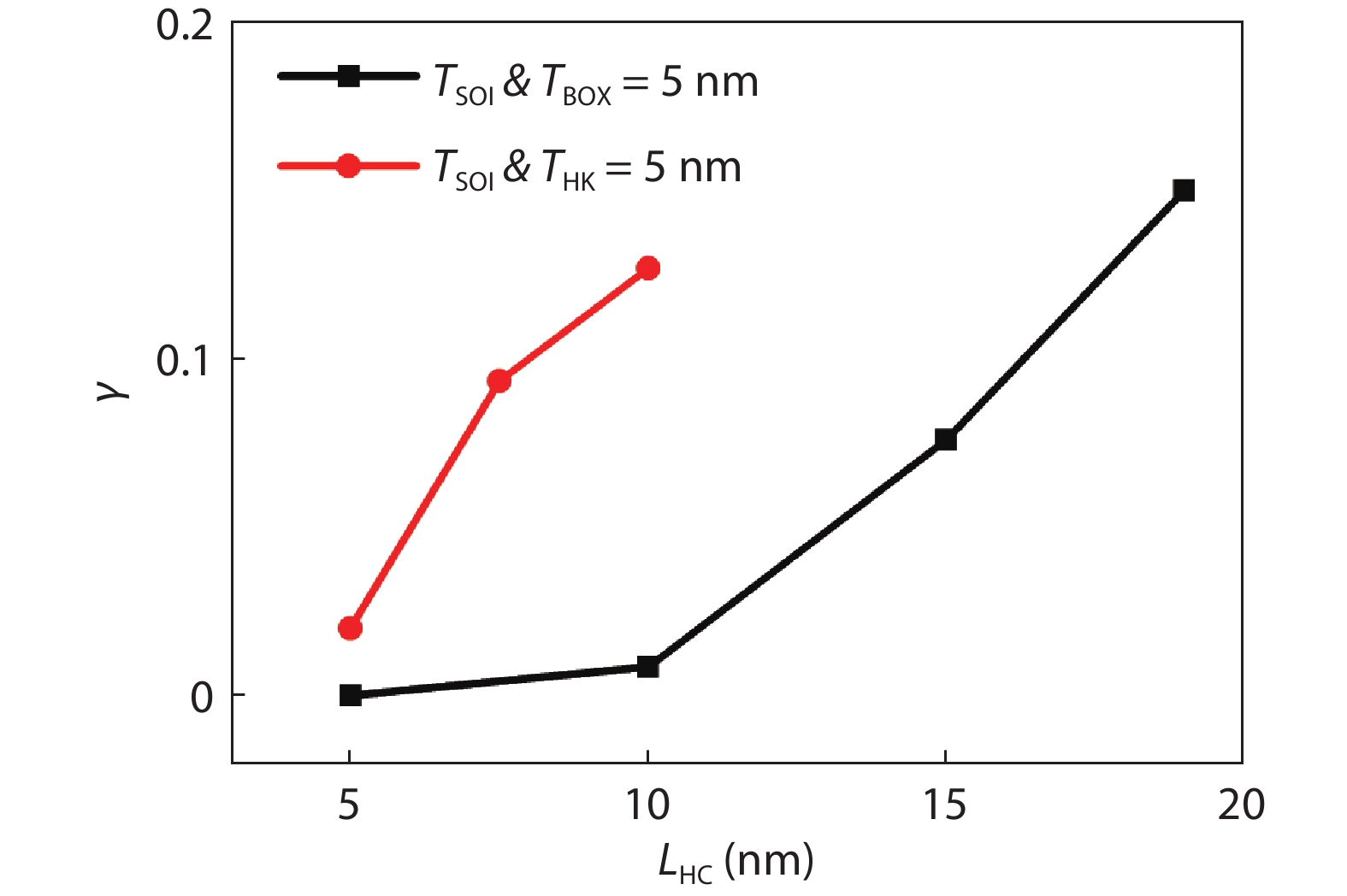
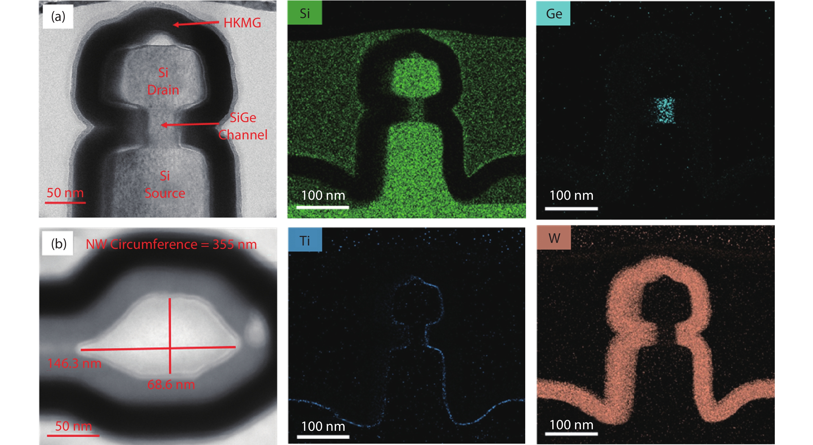
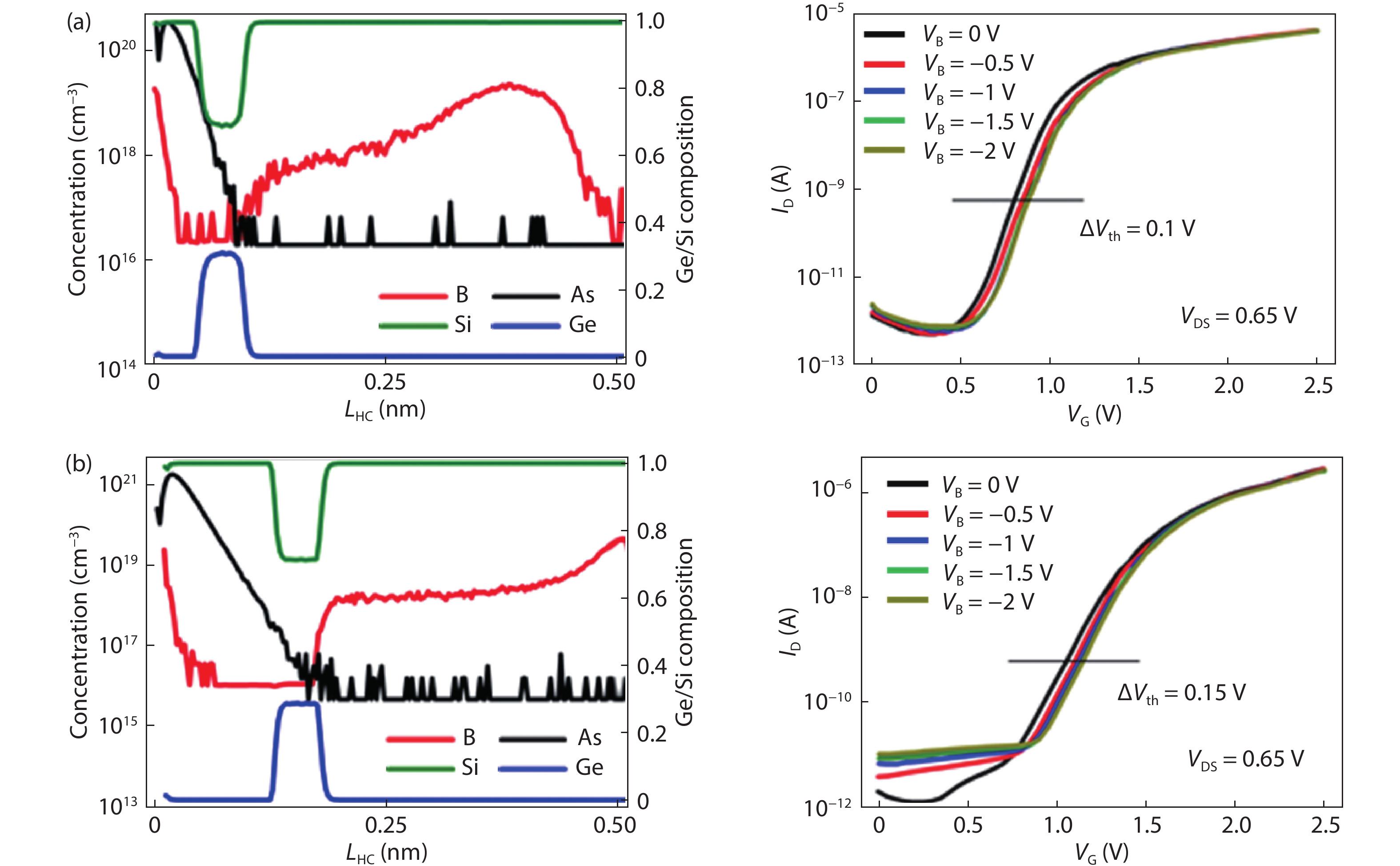
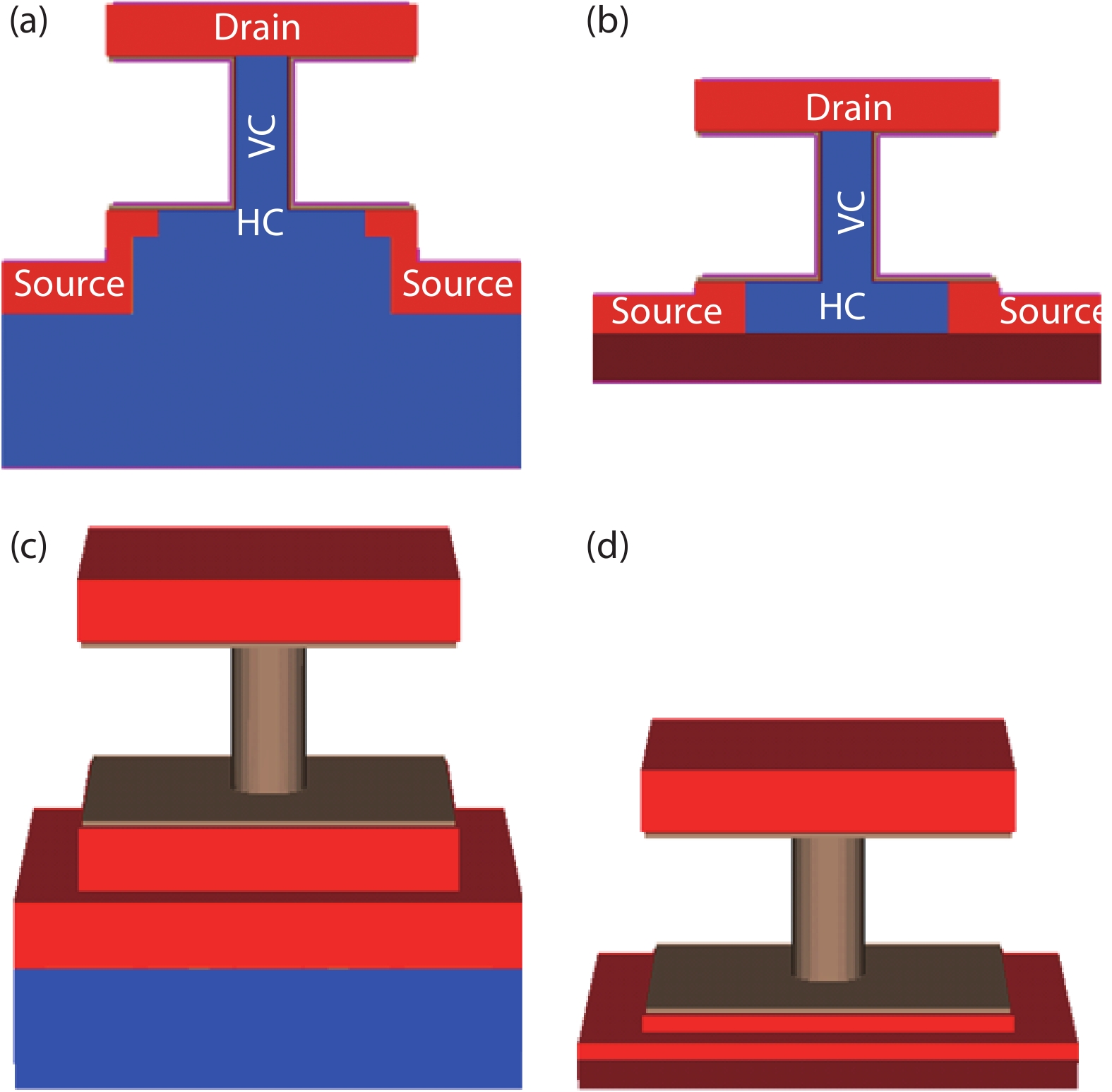
| [1] |
Hisamoto D, Lee W C, Kedzierski J, et al. FinFET – a self-aligned double-gate MOSFET scalable to 20 nm. IEEE Trans Electron Devices, 2000, 47, 2320 doi: 10.1109/16.887014 |
| [2] |
Loubet N, Hook T, Montanini P, et al. Stacked nanosheet gate-all-around transistor to enable scaling beyond FinFET. 2017 Symposium on VLSI Technology, 2017, 230 doi: 10.23919/VLSIT.2017.7998183 |
| [3] |
Ritzenthaler R, Mertens H, Pena V, et al. Vertically stacked gate-all-around Si nanowire CMOS transistors with reduced vertical nanowires separation, new work function metal gate solutions, and DC/AC performance optimization. 2018 IEEE International Electron Devices Meeting (IEDM), 2018, 21.5.1 doi: 10.1109/IEDM.2018.8614528 |
| [4] |
|
| [5] |
Yakimets D, Eneman G, Schuddinck P, et al. Vertical GAAFETs for the ultimate CMOS scaling. IEEE Trans Electron Devices, 2015, 62, 1433 doi: 10.1109/TED.2015.2414924 |
| [6] |
Pan C Y, Raghavan P, Yakimets D, et al. Technology/system codesign and benchmarking for lateral and vertical GAA nanowire FETs at 5-nm technology node. IEEE Trans Electron Devices, 2015, 62, 3125 doi: 10.1109/TED.2015.2461457 |
| [7] |
Kwong D L, Li X, Sun Y, et al. Vertical silicon nanowire platform for low power electronics and clean energy applications. J Nanotechnol, 2012, 2012, 1 doi: 10.1155/2012/492121 |
| [8] |
Veloso A, Altamirano-Sanchez E, Brus S, et al. Vertical nanowire FET integration and device aspects. ECS Trans, 2016, 72, 31 doi: 10.1149/07204.0031ecst |
| [9] |
Bohr M , Fellow I S . Silicon technology leadership for the mobility era. Intel Developer Forum, 2012
|
| [10] |
Choi Y K, Chang L, Ranade P, et al. FinFET process refinements for improved mobility and gate work function engineering. Dig Int Electron Devices Meet, 2002, 259 doi: 10.1109/IEDM.2002.1175827 |
| [11] |
Pherson M R M. The adjustment of mos transistor threshold voltage by ion implantation. Appl Phys Lett, 1971, 18, 502 doi: 10.1063/1.1653513 |
| [12] |
Lee T, Rhee S J, Kang C, et al. Structural advantage for the EOT scaling and improved electron channel mobility by incorporating dysprosium oxide (Dy 2O 3) into HfO 2 n-MOSFETs. IEEE Electron Device Lett, 2006, 27, 640 doi: 10.1109/LED.2006.879023 |
| [13] |
Park J W, Baik H K, Lim T, et al. Threshold voltage control of oxide nanowire transistors using nitrogen plasma treatment. Appl Phys Lett, 2010, 97, 203508 doi: 10.1063/1.3518485 |
| [14] |
Fried D M, Duster J S, Kornegay K T. Improved independent gate N-type FinFET fabrication and characterization. IEEE Electron Device Lett, 2003, 24, 592 doi: 10.1109/LED.2003.815946 |
| [15] |
Denton J P, Neudeck G W. Fully depleted dual-gated thin-film SOI P-MOSFETs fabricated in SOI islands with an isolated buried polysilicon backgate. IEEE Electron Device Lett, 1996, 17, 509 doi: 10.1109/55.541764 |
| [16] |
Liu Y X, Masahara M, Ishii K, et al. Flexible threshold voltage FinFETs with independent double gates and an ideal rectangular cross-section Si-Fin channel. IEEE International Electron Devices Meeting, 2003, 18.8.1 doi: 10.1109/IEDM.2003.1269445 |
| [17] |
Fried D M, Duster J S, Kornegay K T. High-performance p-type independent-gate FinFETs. IEEE Electron Device Lett, 2004, 25, 199 doi: 10.1109/LED.2004.825160 |
| [18] |
Kumar M P V, Lin J Y, Kao K H, et al. Junctionless FETs with a fin body for multi- VTH and dynamic threshold operation. IEEE Trans Electron Devices, 2018, 65, 3535 doi: 10.1109/TED.2018.2847355 |
| [19] |
Ota K, Saitoh M, Tanaka C, et al. Threshold voltage control by substrate bias in 10-nm-diameter tri-gate nanowire MOSFET on ultrathin BOX. IEEE Electron Device Lett, 2013, 34, 187 doi: 10.1109/LED.2012.2234719 |
| [20] |
Ohtou T, Saraya T, Hiramoto T. Variable-body-factor SOI MOSFET with ultrathin buried oxide for adaptive threshold voltage and leakage control. IEEE Trans Electron Devices, 2008, 55, 40 doi: 10.1109/TED.2007.912612 |
| [21] |
Pelloux-Prayer B, Blagojevi? M, Thomas O, et al. Planar fully depleted SOI technology: The convergence of high performance and low power towards multimedia mobile applications. 2012 IEEE Faible Tension Faible Consommation, 2012, 1 doi: 10.1109/FTFC.2012.6231742 |
| [22] |
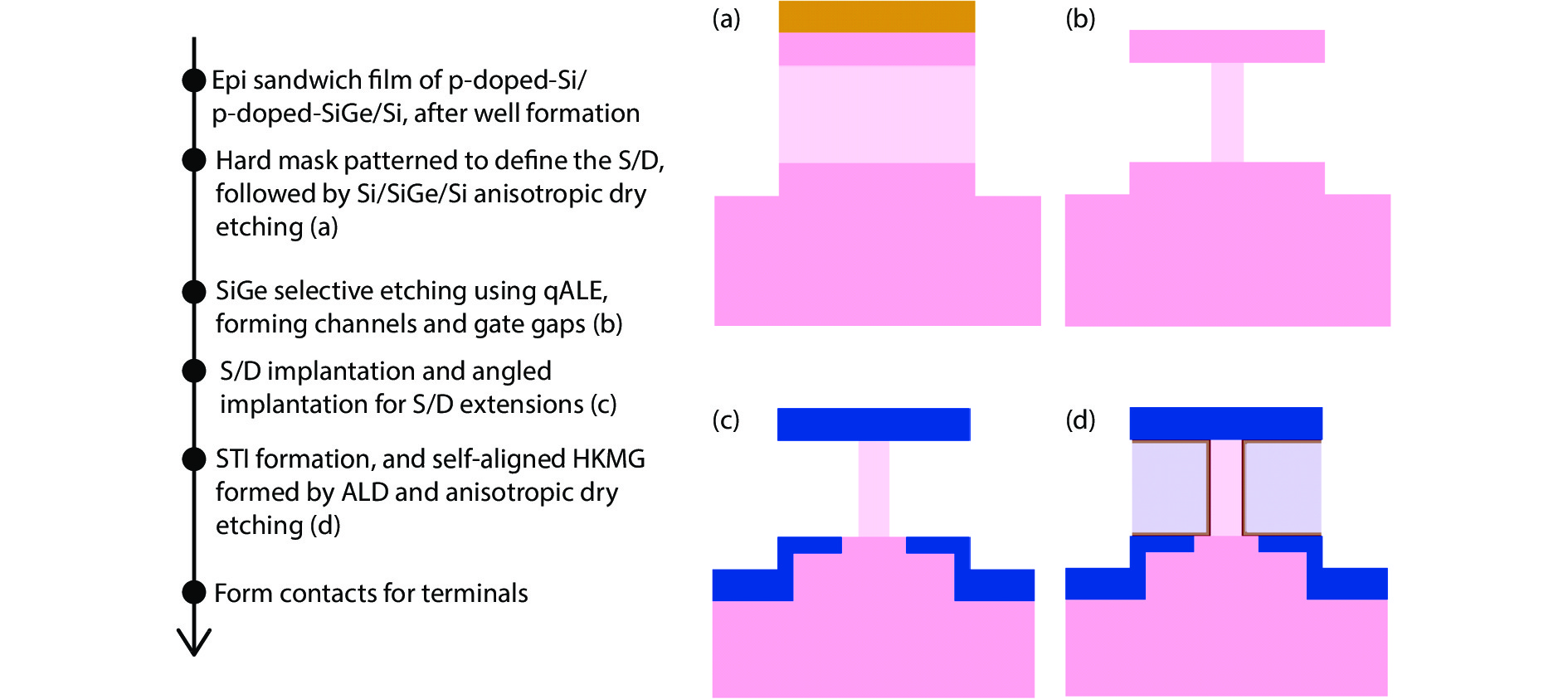
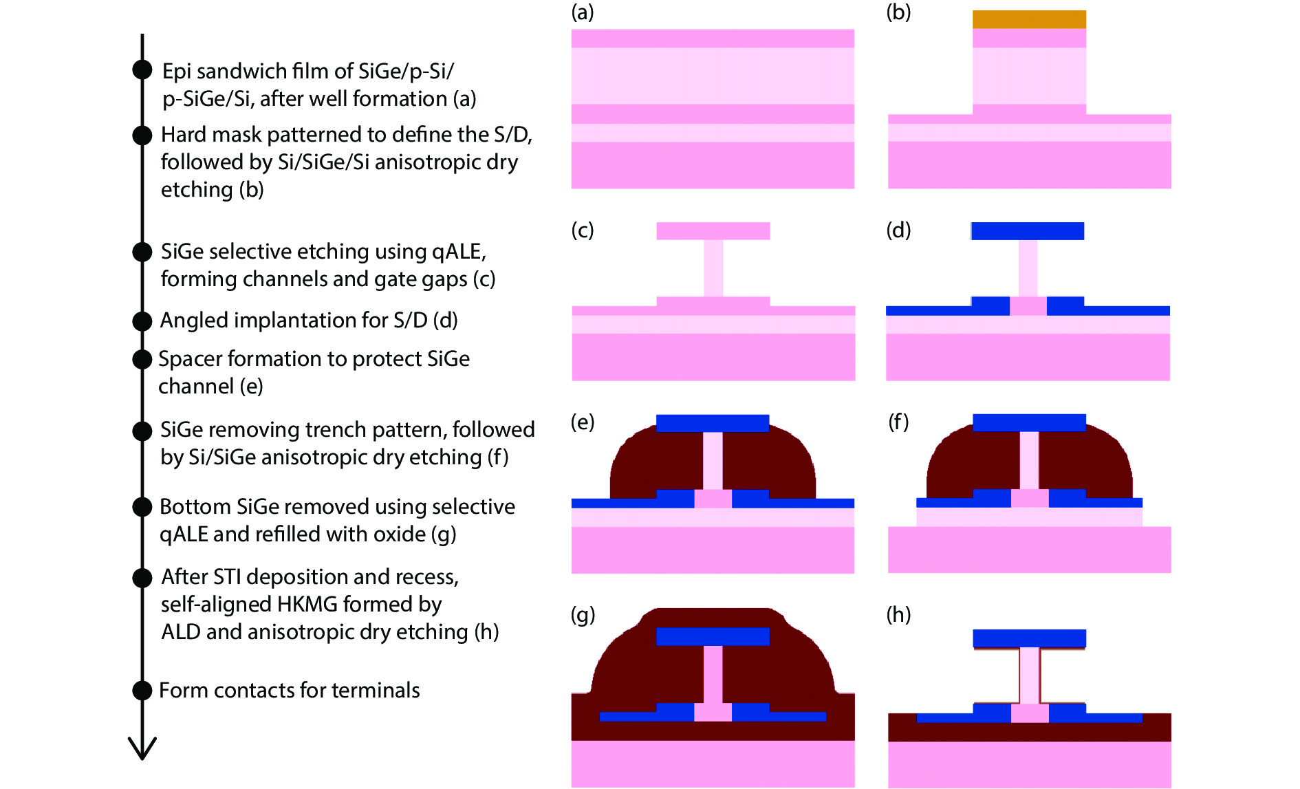
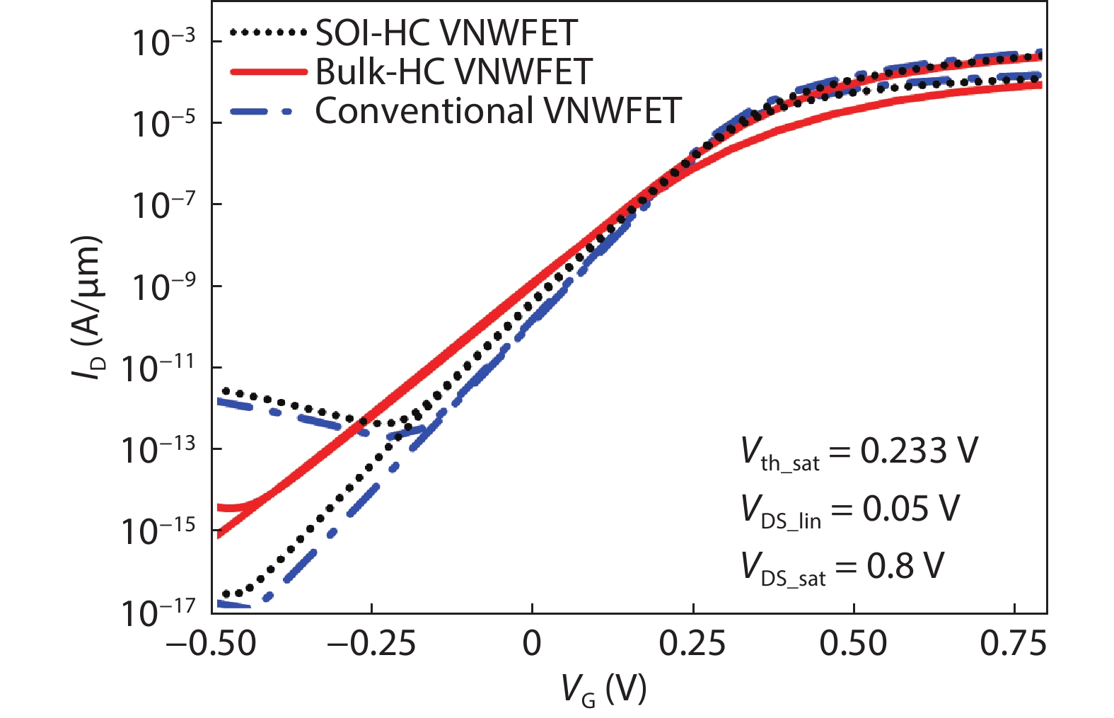
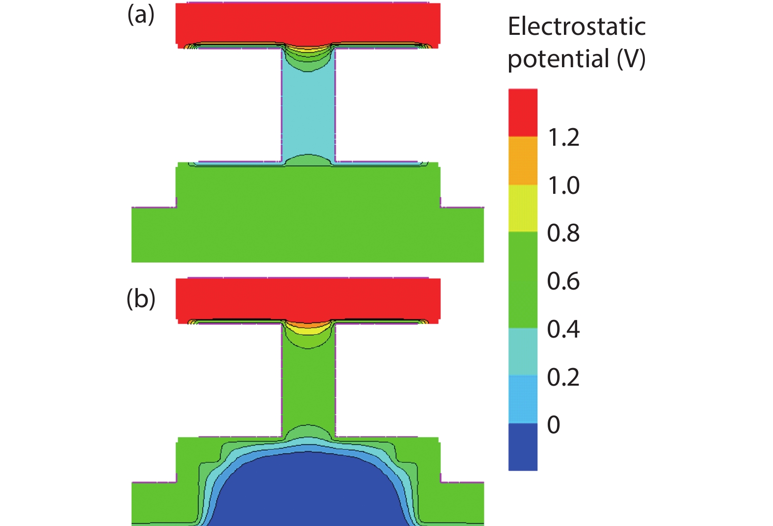
Yin X G, Zhang Y K, Zhu H L, et al. Vertical sandwich gate-all-around field-effect transistors with self-aligned high-k metal gates and small effective-gate-length variation. IEEE Electron Device Lett, 2020, 41, 8 doi: 10.1109/LED.2019.2954537 |
| [23] |
Yin X G, Zhu H L, Zhao L H, et al. Study of isotropic and Si-selective quasi atomic layer etching of Si 1– xGe x. ECS J Solid State Sci Technol, 2020, 9, 034012 doi: 10.1149/2162-8777/ab80ae |


 DownLoad: