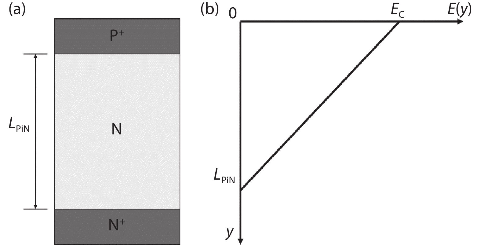
Fig. 1.
(a) A typical P–i–N structure. (b) Electric field distribution.
REVIEWS
Run Tian1, 2, Chao Ma3, , Jingmin Wu1, 2, Zhiyu Guo1, 2, Xiang Yang1 and Zhongchao Fan1, 4,
Corresponding author: Chao Ma, machao@ime.ac.cn; Zhongchao Fan, zcfan@semi.ac.cn
Abstract: Superjunction technology is believed to reach the optimal specific on-resistance and breakdown voltage trade-off. It has become a mainstream technology in silicon high-voltage metal oxide semiconductor field effect transistor devices. Numerous efforts have been conducted to employ the same concept in silicon carbide devices. These works are summarized here.
Key words: silicon carbide (SiC), power semiconductor devices, superjunction (SJ), process development
| [1] |
Baliga B J. Trends in power semiconductor devices. IEEE Trans Electron Devices, 1996, 43(10), 1717 doi: 10.1109/16.536818
|
| [2] |
Huang A Q. Power semiconductor devices for smart grid and renewable energy systems. J Proc IEEE, 2017, 105(11), 2019 doi: 10.1109/JPROC.2017.2687701
|
| [3] |
Baliga B J. Fundamentals of power semiconductor devices. New York: Springer Verlag, 2008
|
| [4] |
Kimoto T, Cooper J A. Fundamentals of silicon carbide technology. Singapore: Wiley, 2014
|
| [5] |
Tsuchida H, Kamata I, Jikimoto T, et al. Epitaxial growth of thick 4H-SiC layers in a vertical radiant-heating reactor. J Cryst Growth, 2002, 237–239, 1206 doi: 10.1557/PROC-640-H2.12
|
| [6] |
Onishi Y, Iwamoto S, Sato T, et al. 24 mΩ·cm2 680 V silicon superjunction MOSFET. International Symposium on Power Semiconductor Devices and ICs, 2002, 241
|
| [7] |
Saito W, Omura I, Aida S, et al. A 20 mΩ·cm2 600 V-class Superjunction MOSFET. International Symposium on Power Semiconductor Devices and ICs, 2004, 459
|
| [8] |
Rub M, Bar M, Deboy G, et al. 550 V superjunction 3.9 Ω·mm2 transistor formed by 25 MeV masked boron implantation. International Symposium on Power Semiconductor Devices and ICs, 2004, 455
|
| [9] |
Yamauchi S, Urakami Y, Tuji N, et al. Defect-less trench filling of epitaxial Si growth by H2 annealing. International Symposium on Power Semiconductor Devices and ICs, 2002, 133
|
| [10] |
Iwamoto S, Takahashi K, Kuribayashi H, et al. Above 500 V class Superjunction MOSFETs fabricated by deep trench etching and epitaxial growth. International Symposium on Power Semiconductor Devices and ICs, 2005, 31
|
| [11] |
Sakakibara J, Noda Y, Shibata T, et al. 600 V-class super junction MOSFET with high aspect ratio P/N columns structure. International Symposium on Power Semiconductor Devices and ICs, 2008, 299
|
| [12] |
Udrea F, Deboy G, Fujihira T. Superjunction power devices, history, development, and future prospects. IEEE Trans Electron Devices, 2017, 64(3), 713 doi: 10.1109/TED.2017.2658344
|
| [13] |
Kobayashi Y, Kyogoku S, Morimoto T, et al. High-temperature performance of 1.2 kV-class SiC super junction MOSFET. International Symposium on Power Semiconductor Devices and ICs, 2019, 31
|
| [14] |
Kosugi R, Sakuma Y, Kojima K, et al. First experimental demonstration of SiC super-junction (SJ) structure by multi-epitaxial growth method. International Symposium on Power Semiconductor Devices and ICs, 2014, 346
|
| [15] |
Rueb M. Addressing production of SiC super-junction MOSFETs. J Compd Semicond, 2019, 25(3), 38
|
| [16] |
Ishibashi N, Fukada K, Bandoh A, et al. High-quality 100/150 mm p-type 4H-SiC epitaxial wafer for high-voltage bipolar devices. Mater Sci Forum, 2017, 897, 55 doi: 10.4028/www.scientific.net/MSF.897.55
|
| [17] |
Ding R X, Yang Y T, Han R. Microtrenching effect of SiC ICP etching in SF6/O2 plasma. J Semicond, 2009, 30(1), 016001 doi: 10.1088/1674-4926/30/1/016001
|
| [18] |
Han C, Zhang Y, Song Q, et al. An improved ICP etching for mesa-terminated 4H-SiC P –i –N diodes. IEEE Trans Electron Devices, 2015, 62(4), 1223 doi: 10.1109/TED.2015.2403615
|
| [19] |
Beheim G M, Evans L J. Control of trenching and surface roughness in deep reactive ion etched 4H and 6H SiC. MRS Proc, 2006, 911, 0911 doi: 10.1557/PROC-0911-B10-15
|
| [20] |
Kimoto T, Yamamoto T, Chen Z Y, et al. 4H-SiC (11-20) epitaxial growth. Mater Sci Forum, 2000, 338–342, 189 doi: 10.4028/www.scientific.net/MSF.338-342.189
|
| [21] |
Takeuchi Y, Kataoka M, Kimoto T, et al. SiC migration enhanced embedded epitaxial (ME3) growth technology. Mater Sci Forum, 2006, 527–529, 251 doi: 10.4028/www.scientific.net/MSF.527-529.251
|
| [22] |
Kimoto T, Matsunami H. Surface diffusion lengths of adatoms on 6H-SiC{0001} faces in chemical vapor deposition of SiC. J Appl Phys, 1995, 78(5), 3132 doi: 10.1063/1.359999
|
| [23] |
Ji S, Kojima K, Kosugi R, et al. Influence of growth pressure on filling 4H-SiC trenches by CVD method. Jpn J Appl Phys, 2016, 55(1S), 01AC04 doi: 10.7567/JJAP.55.01AC04
|
| [24] |
Ji S, Kojima K, Kosugi R, et al. Filling 4H-SiC trench towards selective epitaxial growth by adding HCl to CVD process. Appl Phys Express, 2015, 8(6), 065502 doi: 10.7567/APEX.8.065502
|
| [25] |
Kosugi R, Ji S, Mochizuki K, et al. Strong impact of slight trench direction misalignment from [11-20] on deep trench filling epitaxy for SiC super-junction devices. Jpn J Appl Phys, 2017, 56(4S), 04CR05 doi: 10.7567/JJAP.56.04CR05
|
| [26] |
Kosugi R, Sakuma Y, Kojima K, et al. Development of SiC super-junction (SJ) device by deep trench-filling epitaxial growth. Mater Sci Forum, 2013, 740–742, 785 doi: 10.4028/www.scientific.net/MSF.740-742.785
|
| [27] |
Kojima K, Nagata A, Ito S, et al. Filling of deep trench by epitaxial SiC growth. Mater Sci Forum, 2013, 742, 793 doi: 10.4028/www.scientific.net/MSF.740-742.793
|
| [28] |
Zhong X, Wang B, Sheng K. Design and experimental demonstration of 1.35 kV SiC super junction Schottky diode. International Symposium on Power Semiconductor Devices and ICs, 2016, 231
|
Table 1. The calculation results of SRIM software.
| Depth (μm) | 1 | 3 | 5 | 10 | 20 | 50 | |
| Ion implantation energy (MeV) | N-doping | 1.1 | 5.4 | 9.6 | 19.4 | 35.5 | 72.5 |
| Al-doping | 1.3 | 7.5 | 16.3 | 38.5 | 75.0 | 165.0 |
 DownLoad: CSV
| [1] |
Baliga B J. Trends in power semiconductor devices. IEEE Trans Electron Devices, 1996, 43(10), 1717 doi: 10.1109/16.536818
|
| [2] |
Huang A Q. Power semiconductor devices for smart grid and renewable energy systems. J Proc IEEE, 2017, 105(11), 2019 doi: 10.1109/JPROC.2017.2687701
|
| [3] |
Baliga B J. Fundamentals of power semiconductor devices. New York: Springer Verlag, 2008
|
| [4] |
Kimoto T, Cooper J A. Fundamentals of silicon carbide technology. Singapore: Wiley, 2014
|
| [5] |
Tsuchida H, Kamata I, Jikimoto T, et al. Epitaxial growth of thick 4H-SiC layers in a vertical radiant-heating reactor. J Cryst Growth, 2002, 237–239, 1206 doi: 10.1557/PROC-640-H2.12
|
| [6] |
Onishi Y, Iwamoto S, Sato T, et al. 24 mΩ·cm2 680 V silicon superjunction MOSFET. International Symposium on Power Semiconductor Devices and ICs, 2002, 241
|
| [7] |
Saito W, Omura I, Aida S, et al. A 20 mΩ·cm2 600 V-class Superjunction MOSFET. International Symposium on Power Semiconductor Devices and ICs, 2004, 459
|
| [8] |
Rub M, Bar M, Deboy G, et al. 550 V superjunction 3.9 Ω·mm2 transistor formed by 25 MeV masked boron implantation. International Symposium on Power Semiconductor Devices and ICs, 2004, 455
|
| [9] |
Yamauchi S, Urakami Y, Tuji N, et al. Defect-less trench filling of epitaxial Si growth by H2 annealing. International Symposium on Power Semiconductor Devices and ICs, 2002, 133
|
| [10] |
Iwamoto S, Takahashi K, Kuribayashi H, et al. Above 500 V class Superjunction MOSFETs fabricated by deep trench etching and epitaxial growth. International Symposium on Power Semiconductor Devices and ICs, 2005, 31
|
| [11] |
Sakakibara J, Noda Y, Shibata T, et al. 600 V-class super junction MOSFET with high aspect ratio P/N columns structure. International Symposium on Power Semiconductor Devices and ICs, 2008, 299
|
| [12] |
Udrea F, Deboy G, Fujihira T. Superjunction power devices, history, development, and future prospects. IEEE Trans Electron Devices, 2017, 64(3), 713 doi: 10.1109/TED.2017.2658344
|
| [13] |
Kobayashi Y, Kyogoku S, Morimoto T, et al. High-temperature performance of 1.2 kV-class SiC super junction MOSFET. International Symposium on Power Semiconductor Devices and ICs, 2019, 31
|
| [14] |
Kosugi R, Sakuma Y, Kojima K, et al. First experimental demonstration of SiC super-junction (SJ) structure by multi-epitaxial growth method. International Symposium on Power Semiconductor Devices and ICs, 2014, 346
|
| [15] |
Rueb M. Addressing production of SiC super-junction MOSFETs. J Compd Semicond, 2019, 25(3), 38
|
| [16] |
Ishibashi N, Fukada K, Bandoh A, et al. High-quality 100/150 mm p-type 4H-SiC epitaxial wafer for high-voltage bipolar devices. Mater Sci Forum, 2017, 897, 55 doi: 10.4028/www.scientific.net/MSF.897.55
|
| [17] |
Ding R X, Yang Y T, Han R. Microtrenching effect of SiC ICP etching in SF6/O2 plasma. J Semicond, 2009, 30(1), 016001 doi: 10.1088/1674-4926/30/1/016001
|
| [18] |
Han C, Zhang Y, Song Q, et al. An improved ICP etching for mesa-terminated 4H-SiC P –i –N diodes. IEEE Trans Electron Devices, 2015, 62(4), 1223 doi: 10.1109/TED.2015.2403615
|
| [19] |
Beheim G M, Evans L J. Control of trenching and surface roughness in deep reactive ion etched 4H and 6H SiC. MRS Proc, 2006, 911, 0911 doi: 10.1557/PROC-0911-B10-15
|
| [20] |
Kimoto T, Yamamoto T, Chen Z Y, et al. 4H-SiC (11-20) epitaxial growth. Mater Sci Forum, 2000, 338–342, 189 doi: 10.4028/www.scientific.net/MSF.338-342.189
|
| [21] |
Takeuchi Y, Kataoka M, Kimoto T, et al. SiC migration enhanced embedded epitaxial (ME3) growth technology. Mater Sci Forum, 2006, 527–529, 251 doi: 10.4028/www.scientific.net/MSF.527-529.251
|
| [22] |
Kimoto T, Matsunami H. Surface diffusion lengths of adatoms on 6H-SiC{0001} faces in chemical vapor deposition of SiC. J Appl Phys, 1995, 78(5), 3132 doi: 10.1063/1.359999
|
| [23] |
Ji S, Kojima K, Kosugi R, et al. Influence of growth pressure on filling 4H-SiC trenches by CVD method. Jpn J Appl Phys, 2016, 55(1S), 01AC04 doi: 10.7567/JJAP.55.01AC04
|
| [24] |
Ji S, Kojima K, Kosugi R, et al. Filling 4H-SiC trench towards selective epitaxial growth by adding HCl to CVD process. Appl Phys Express, 2015, 8(6), 065502 doi: 10.7567/APEX.8.065502
|
| [25] |
Kosugi R, Ji S, Mochizuki K, et al. Strong impact of slight trench direction misalignment from [11-20] on deep trench filling epitaxy for SiC super-junction devices. Jpn J Appl Phys, 2017, 56(4S), 04CR05 doi: 10.7567/JJAP.56.04CR05
|
| [26] |
Kosugi R, Sakuma Y, Kojima K, et al. Development of SiC super-junction (SJ) device by deep trench-filling epitaxial growth. Mater Sci Forum, 2013, 740–742, 785 doi: 10.4028/www.scientific.net/MSF.740-742.785
|
| [27] |
Kojima K, Nagata A, Ito S, et al. Filling of deep trench by epitaxial SiC growth. Mater Sci Forum, 2013, 742, 793 doi: 10.4028/www.scientific.net/MSF.740-742.793
|
| [28] |
Zhong X, Wang B, Sheng K. Design and experimental demonstration of 1.35 kV SiC super junction Schottky diode. International Symposium on Power Semiconductor Devices and ICs, 2016, 231
|


Article views: 6107 Times PDF downloads: 469 Times Cited by: 0 Times
Received: 23 September 2020 Revised: 09 November 2020 Online: Accepted Manuscript: 28 December 2020Uncorrected proof: 29 December 2020Published: 01 June 2021
| Citation: |
Run Tian, Chao Ma, Jingmin Wu, Zhiyu Guo, Xiang Yang, Zhongchao Fan. A review of manufacturing technologies for silicon carbide superjunction devices[J]. Journal of Semiconductors, 2021, 42(6): 061801. doi: 10.1088/1674-4926/42/6/061801
****
R Tian, C Ma, J M Wu, Z Y Guo, X Yang, Z C Fan, A review of manufacturing technologies for silicon carbide superjunction devices[J]. J. Semicond., 2021, 42(6): 061801. doi: 10.1088/1674-4926/42/6/061801.

|
| [1] |
Baliga B J. Trends in power semiconductor devices. IEEE Trans Electron Devices, 1996, 43(10), 1717 doi: 10.1109/16.536818
|
| [2] |
Huang A Q. Power semiconductor devices for smart grid and renewable energy systems. J Proc IEEE, 2017, 105(11), 2019 doi: 10.1109/JPROC.2017.2687701
|
| [3] |
Baliga B J. Fundamentals of power semiconductor devices. New York: Springer Verlag, 2008
|
| [4] |
Kimoto T, Cooper J A. Fundamentals of silicon carbide technology. Singapore: Wiley, 2014
|
| [5] |
Tsuchida H, Kamata I, Jikimoto T, et al. Epitaxial growth of thick 4H-SiC layers in a vertical radiant-heating reactor. J Cryst Growth, 2002, 237–239, 1206 doi: 10.1557/PROC-640-H2.12
|
| [6] |
Onishi Y, Iwamoto S, Sato T, et al. 24 mΩ·cm2 680 V silicon superjunction MOSFET. International Symposium on Power Semiconductor Devices and ICs, 2002, 241
|
| [7] |
Saito W, Omura I, Aida S, et al. A 20 mΩ·cm2 600 V-class Superjunction MOSFET. International Symposium on Power Semiconductor Devices and ICs, 2004, 459
|
| [8] |
Rub M, Bar M, Deboy G, et al. 550 V superjunction 3.9 Ω·mm2 transistor formed by 25 MeV masked boron implantation. International Symposium on Power Semiconductor Devices and ICs, 2004, 455
|
| [9] |
Yamauchi S, Urakami Y, Tuji N, et al. Defect-less trench filling of epitaxial Si growth by H2 annealing. International Symposium on Power Semiconductor Devices and ICs, 2002, 133
|
| [10] |
Iwamoto S, Takahashi K, Kuribayashi H, et al. Above 500 V class Superjunction MOSFETs fabricated by deep trench etching and epitaxial growth. International Symposium on Power Semiconductor Devices and ICs, 2005, 31
|
| [11] |
Sakakibara J, Noda Y, Shibata T, et al. 600 V-class super junction MOSFET with high aspect ratio P/N columns structure. International Symposium on Power Semiconductor Devices and ICs, 2008, 299
|
| [12] |
Udrea F, Deboy G, Fujihira T. Superjunction power devices, history, development, and future prospects. IEEE Trans Electron Devices, 2017, 64(3), 713 doi: 10.1109/TED.2017.2658344
|
| [13] |
Kobayashi Y, Kyogoku S, Morimoto T, et al. High-temperature performance of 1.2 kV-class SiC super junction MOSFET. International Symposium on Power Semiconductor Devices and ICs, 2019, 31
|
| [14] |
Kosugi R, Sakuma Y, Kojima K, et al. First experimental demonstration of SiC super-junction (SJ) structure by multi-epitaxial growth method. International Symposium on Power Semiconductor Devices and ICs, 2014, 346
|
| [15] |
Rueb M. Addressing production of SiC super-junction MOSFETs. J Compd Semicond, 2019, 25(3), 38
|
| [16] |
Ishibashi N, Fukada K, Bandoh A, et al. High-quality 100/150 mm p-type 4H-SiC epitaxial wafer for high-voltage bipolar devices. Mater Sci Forum, 2017, 897, 55 doi: 10.4028/www.scientific.net/MSF.897.55
|
| [17] |
Ding R X, Yang Y T, Han R. Microtrenching effect of SiC ICP etching in SF6/O2 plasma. J Semicond, 2009, 30(1), 016001 doi: 10.1088/1674-4926/30/1/016001
|
| [18] |
Han C, Zhang Y, Song Q, et al. An improved ICP etching for mesa-terminated 4H-SiC P –i –N diodes. IEEE Trans Electron Devices, 2015, 62(4), 1223 doi: 10.1109/TED.2015.2403615
|
| [19] |
Beheim G M, Evans L J. Control of trenching and surface roughness in deep reactive ion etched 4H and 6H SiC. MRS Proc, 2006, 911, 0911 doi: 10.1557/PROC-0911-B10-15
|
| [20] |
Kimoto T, Yamamoto T, Chen Z Y, et al. 4H-SiC (11-20) epitaxial growth. Mater Sci Forum, 2000, 338–342, 189 doi: 10.4028/www.scientific.net/MSF.338-342.189
|
| [21] |
Takeuchi Y, Kataoka M, Kimoto T, et al. SiC migration enhanced embedded epitaxial (ME3) growth technology. Mater Sci Forum, 2006, 527–529, 251 doi: 10.4028/www.scientific.net/MSF.527-529.251
|
| [22] |
Kimoto T, Matsunami H. Surface diffusion lengths of adatoms on 6H-SiC{0001} faces in chemical vapor deposition of SiC. J Appl Phys, 1995, 78(5), 3132 doi: 10.1063/1.359999
|
| [23] |
Ji S, Kojima K, Kosugi R, et al. Influence of growth pressure on filling 4H-SiC trenches by CVD method. Jpn J Appl Phys, 2016, 55(1S), 01AC04 doi: 10.7567/JJAP.55.01AC04
|
| [24] |
Ji S, Kojima K, Kosugi R, et al. Filling 4H-SiC trench towards selective epitaxial growth by adding HCl to CVD process. Appl Phys Express, 2015, 8(6), 065502 doi: 10.7567/APEX.8.065502
|
| [25] |
Kosugi R, Ji S, Mochizuki K, et al. Strong impact of slight trench direction misalignment from [11-20] on deep trench filling epitaxy for SiC super-junction devices. Jpn J Appl Phys, 2017, 56(4S), 04CR05 doi: 10.7567/JJAP.56.04CR05
|
| [26] |
Kosugi R, Sakuma Y, Kojima K, et al. Development of SiC super-junction (SJ) device by deep trench-filling epitaxial growth. Mater Sci Forum, 2013, 740–742, 785 doi: 10.4028/www.scientific.net/MSF.740-742.785
|
| [27] |
Kojima K, Nagata A, Ito S, et al. Filling of deep trench by epitaxial SiC growth. Mater Sci Forum, 2013, 742, 793 doi: 10.4028/www.scientific.net/MSF.740-742.793
|
| [28] |
Zhong X, Wang B, Sheng K. Design and experimental demonstration of 1.35 kV SiC super junction Schottky diode. International Symposium on Power Semiconductor Devices and ICs, 2016, 231
|

 WeChat ID
Journal of Semiconductors © 2017 All Rights Reserved 京ICP備05085259號-2