


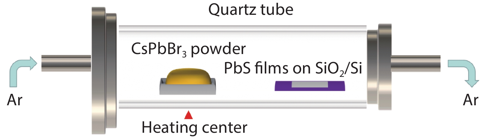
Fig. 1.
(Color online) Schematic diagram of the tube furnace setup for the growth of CsPbBr3/PbS heterostructures.
ARTICLES
Yifan Wang1, 2, Xuanze Li1, 2, Pei Liu1, 2, Jing Xia1, 2, and Xiangmin Meng1, 2,
Corresponding author: Jing Xia, xiajing@mail.ipc.ac.cn; Xiangmin Meng, mengxiangmin@mail.ipc.ac.cn
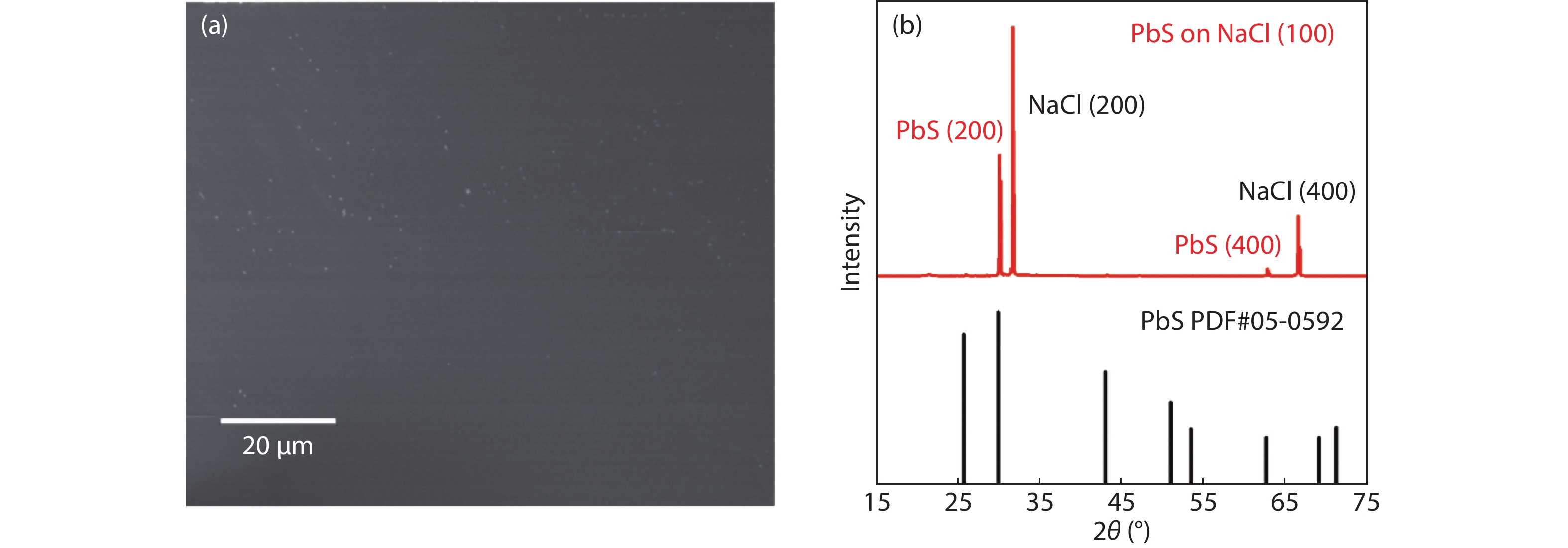
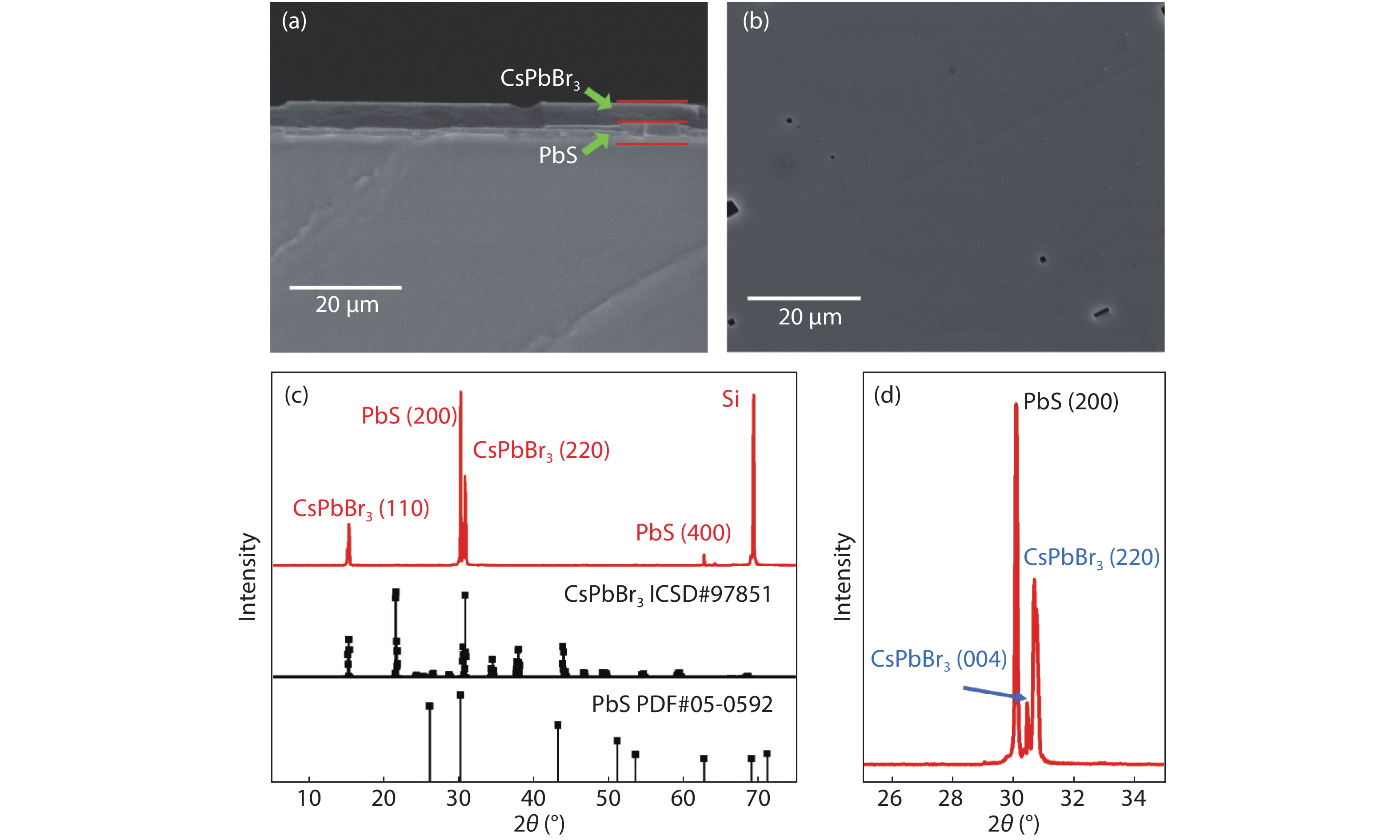
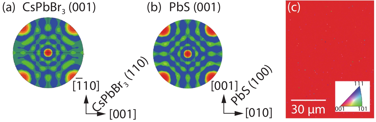
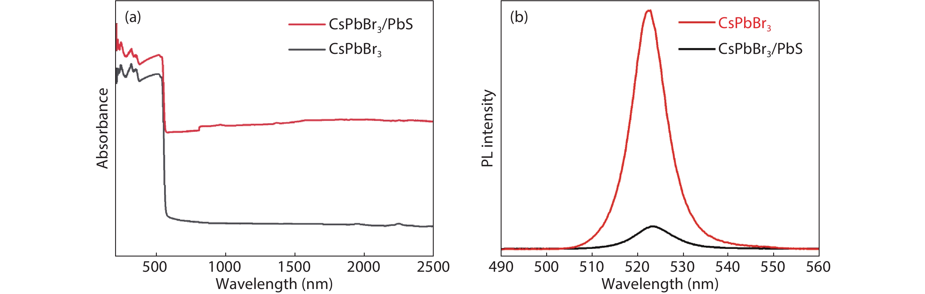
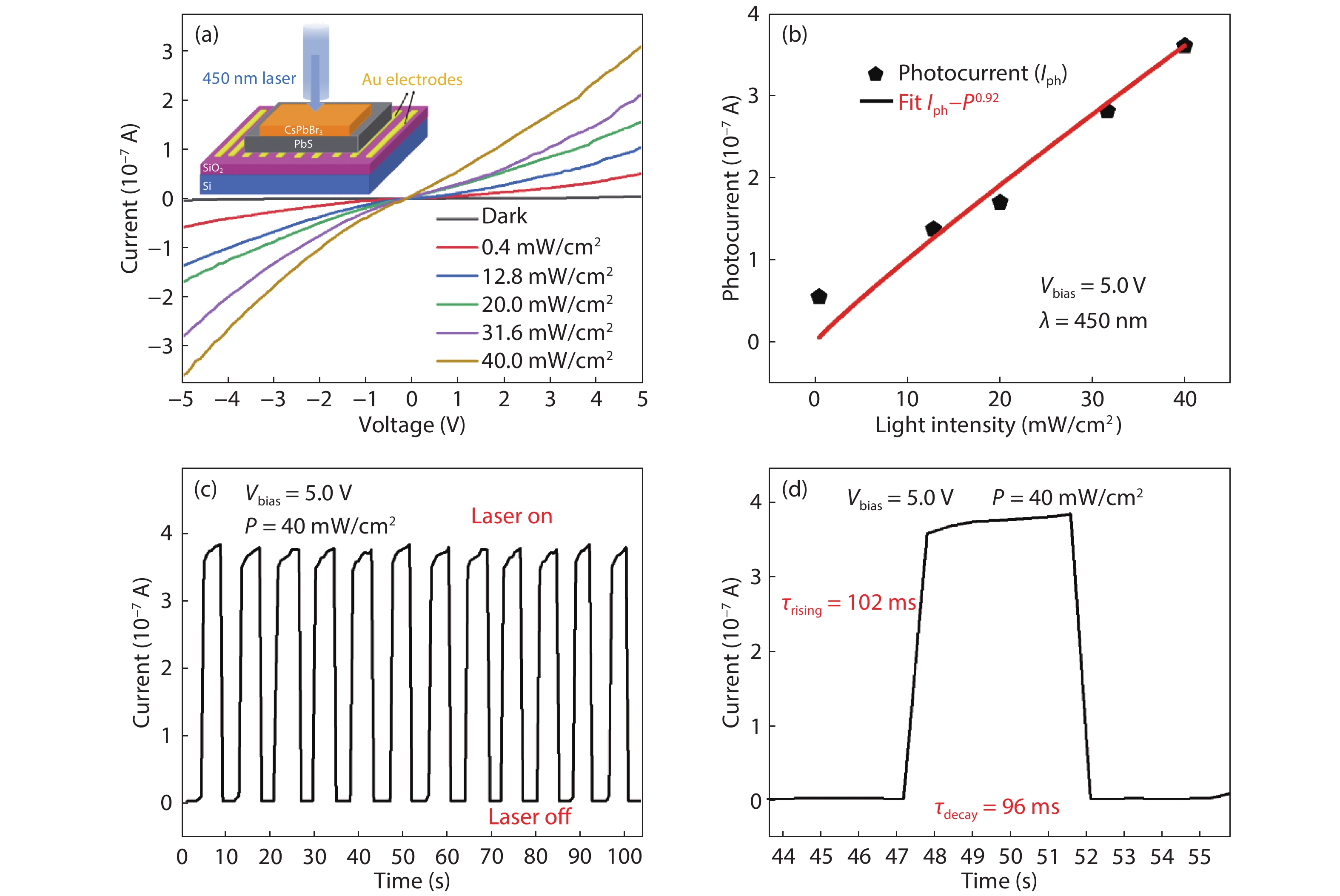
Abstract: Epitaxial high-crystallization film semiconductor heterostructures has been proved to be an effective method to prepare single-crystal films for different functional devices in modern microelectronics, electro-optics, and optoelectronics. With superior semiconducting properties, halide perovskite materials are rising as building blocks for heterostructures. Here, the conformal vapor phase epitaxy of CsPbBr3 on PbS single-crystal films is realized to form the CsPbBr3/PbS heterostructures via a two-step vapor deposition process. The structural characterization reveals that PbS substrates and the epilayer CsPbBr3 have clear relationships: CsPbBr3(110) // PbS(100), CsPbBr3[
Key words: heteroepitaxial growth, CsPbBr3, PbS, single-crystal film, photodetector
| [1] |
Zhao J J, Li H H, Qiu Y C, et al. Programmable single-crystalline PbI2 microplate arrays and their organic/inorganic heterojunctions. Adv Funct Mater, 2020, 30, 2003631 doi: 10.1002/adfm.202003631
|
| [2] |
Xia X H, Tu J P, Zhang Y Q, et al. High-quality metal oxide core/shell nanowire arrays on conductive substrates for electrochemical energy storage. ACS Nano, 2012, 6, 5531 doi: 10.1021/nn301454q
|
| [3] |
Iannaccone G, Bonaccorso F, Colombo L, et al. Quantum engineering of transistors based on 2D materials heterostructures. Nat Nanotechnol, 2018, 13, 183 doi: 10.1038/s41565-018-0082-6
|
| [4] |
Zhang H, Jiang X T, Wang Y L, et al. Preface to the special issue on monoelemental 2D semiconducting materials and their applications. J Semicond, 2020, 41, 080101 doi: 10.1088/1674-4926/41/8/080101
|
| [5] |
Yuan J, Sun T, Hu Z X, et al. Wafer-scale fabrication of two-dimensional PtS2/PtSe2 heterojunctions for efficient and broad band photodetection. ACS Appl Mater Interfaces, 2018, 10, 40614 doi: 10.1021/acsami.8b13620
|
| [6] |
Capasso F. Band-gap engineering: From physics and materials to new semiconductor devices. Science, 1987, 235, 172 doi: 10.1126/science.235.4785.172
|
| [7] |
Zhou J S, Yang J H, Wei Z M. Photodetectors based on 2D material/Si heterostructure. J Semicond, 2020, 41, 080401 doi: 10.1088/1674-4926/41/8/080401
|
| [8] |
Kroemer H. A proposed class of hetero-junction injection lasers. Proc IEEE, 1963, 51, 1782
|
| [9] |
Feng M, Holonyak N, Chan R. Quantum-well-base heterojunction bipolar light-emitting transistor. Appl Phys Lett, 2004, 84, 1952 doi: 10.1063/1.1669071
|
| [10] |
Lee K, Li J, Cheng L, et al. Sub-picosecond carrier dynamics induced by efficient charge transfer in MoTe2/WTe2 van der Waals heterostructures. ACS Nano, 2019, 13, 9587 doi: 10.1021/acsnano.9b04701
|
| [11] |
Zhang P, Zhang Y W, Wei Y, et al. Contact engineering for two-dimensional semiconductors. J Semicond, 2020, 41, 071901 doi: 10.1088/1674-4926/41/7/071901
|
| [12] |
Duan X D, Wang C, Shaw J C, et al. Lateral epitaxial growth of two-dimensional layered semiconductor heterojunctions. Nat Nanotechnol, 2014, 9, 1024 doi: 10.1038/nnano.2014.222
|
| [13] |
Caroff P, Wagner J B, Dick K A, et al. High-quality InAs/InSb nanowire heterostructures grown by metal-organic vapor-phase epitaxy. Small, 2008, 4, 878 doi: 10.1002/smll.200700892
|
| [14] |
Liu Y, Huang Y, Duan X F. Van der Waals integration before and beyond two-dimensional materials. Nature, 2019, 567, 323 doi: 10.1038/s41586-019-1013-x
|
| [15] |
Jariwala D, Marks T J, Hersam M C. Mixed-dimensional van der Waals heterostructures. Nat Mater, 2017, 16, 170 doi: 10.1038/nmat4703
|
| [16] |
Zhou S Y, Peng B. Non-volatile optical memory in vertical van der Waals heterostructures. J Semicond, 2020, 41, 072906 doi: 10.1088/1674-4926/41/7/072906
|
| [17] |
Qian F, Li Y, Grade?ak S, et al. Multi-quantum-well nanowire heterostructures for wavelength-controlled lasers. Nat Mater, 2008, 7, 701 doi: 10.1038/nmat2253
|
| [18] |
Walsh A, Scanlon D O, Chen S Y, et al. Self-regulation mechanism for charged point defects in hybrid halide perovskites. Angew Chem Int Ed, 2015, 54, 1791 doi: 10.1002/anie.201409740
|
| [19] |
Gao Y, Zhao L Y, Shang Q Y, et al. Photoluminescence properties of ultrathin CsPbCl3 nanowires on mica substrate. J Semicond, 2019, 40, 052201 doi: 10.1088/1674-4926/40/5/052201
|
| [20] |
Chen H M, Huang W, Marks T J, et al. Recent advances in multi-layer light-emitting heterostructure transistors. Small, 2021, 17, 2007661 doi: 10.1002/smll.202007661
|
| [21] |
Huo N J, Kang J, Wei Z M, et al. Novel and enhanced optoelectronic performances of multilayer MoS2-WS2 heterostructure transistors. Adv Funct Mater, 2014, 24, 7025 doi: 10.1002/adfm.201401504
|
| [22] |
Wang Y P, Chen Z Z, Deschler F, et al. Epitaxial halide perovskite lateral double heterostructure. ACS Nano, 2017, 11, 3355 doi: 10.1021/acsnano.7b00724
|
| [23] |
Yang S J, Liu K L, Han W, et al. Salt-assisted growth of P-type Cu9S5 nanoflakes for P-N heterojunction photodetectors with high responsivity. Adv Funct Mater, 2020, 30, 1908382 doi: 10.1002/adfm.201908382
|
| [24] |
Feng J G, Yan X X, Liu Y, et al. Crystallographically aligned perovskite structures for high-performance polarization-sensitive photodetectors. Adv Mater, 2017, 29, 1605993 doi: 10.1002/adma.201605993
|
| [25] |
Wang Y F, Yang F, Li X Z, et al. Epitaxial growth of large-scale orthorhombic CsPbBr3 perovskite thin films with anisotropic photoresponse property. Adv Funct Mater, 2019, 29, 1904913 doi: 10.1002/adfm.201904913
|
| [26] |
Zhang X L, Xu B, Zhang J B, et al. All-inorganic perovskite nanocrystals for high-efficiency light emitting diodes: Dual-phase CsPbBr3-CsPb2Br5 composites. Adv Funct Mater, 2016, 26, 4595 doi: 10.1002/adfm.201600958
|
| [27] |
Liu C, Li W Z, Zhang C L, et al. All-inorganic CsPbI2Br perovskite solar cells with high efficiency exceeding 13%. J Am Chem Soc, 2018, 140, 3825 doi: 10.1021/jacs.7b13229
|
| [28] |
Huang L, Huo N J, Zheng Z Q, et al. Two-dimensional transition metal dichalcogenides for lead halide perovskites-based photodetectors: Band alignment investigation for the case of CsPbBr3/MoSe2. J Semicond, 2020, 41, 052206 doi: 10.1088/1674-4926/41/5/052206
|
| [29] |
Zhou Q W, Duan J L, Yang X Y, et al. Interfacial strain release from the WS2/CsPbBr3 van der waals heterostructure for 1.7?V voltage all-inorganic perovskite solar cells. Angew Chem Int Ed, 2020, 59, 21997 doi: 10.1002/anie.202010252
|
| [30] |
Jiang J, Sun X, Chen X C, et al. Carrier lifetime enhancement in halide perovskite via remote epitaxy. Nat Commun, 2019, 10, 4145 doi: 10.1038/s41467-019-12056-1
|
| [31] |
Song X F, Liu X H, Yu D J, et al. Boosting two-dimensional MoS2/CsPbBr3 photodetectors via enhanced light absorbance and interfacial carrier separation. ACS Appl Mater Interfaces, 2018, 10, 2801 doi: 10.1021/acsami.7b14745
|
| [32] |
Huo N J, Yang Y J, Li J B. Optoelectronics based on 2D TMDs and heterostructures. J Semicond, 2017, 38, 031002 doi: 10.1088/1674-4926/38/3/031002
|
| [33] |
Li Z J, Hofman E, Li J, et al. Photoelectrochemically active and environmentally stable CsPbBr3/TiO2 core/shell nanocrystals. Adv Funct Mater, 2018, 28, 1704288 doi: 10.1002/adfm.201704288
|
| [34] |
Zhong Q X, Cao M H, Hu H C, et al. One-pot synthesis of highly stable CsPbBr3@SiO2 core–shell nanoparticles. ACS Nano, 2018, 12, 8579 doi: 10.1021/acsnano.8b04209
|
| [35] |
Fan C, Xu X, Yang K, et al. Controllable epitaxial growth of core-shell PbSe@CsPbBr3 wire heterostructures. Adv Mater, 2018, 30, 1804707 doi: 10.1002/adma.201804707
|
| [36] |
Liu Q B, Liang L H, Shen H Z, et al. Epitaxial growth of CsPbBr3-PbS vertical and lateral heterostructures for visible to infrared broadband photodetection. Nano Res, 2021, 14, 1 doi: 10.1007/s12274-021-3308-0
|
| [37] |
Wei Z, Perumal A, Su R, et al. Solution-processed highly bright and durable cesium lead halide perovskite light-emitting diodes. Nanoscale, 2016, 8, 18021 doi: 10.1039/C6NR05330K
|
| [38] |
Zhang X J, Wu X X, Liu X Y, et al. Heterostructural CsPbX3-PbS (X = Cl, Br, I) quantum dots with tunable vis-NIR dual emission. J Am Chem Soc, 2020, 142, 4464 doi: 10.1021/jacs.9b13681
|
| [39] |
Shen Y D, Chen R J, Yu X C, et al. Gibbs-Thomson effect in planar nanowires: Orientation and doping modulated growth. Nano Lett, 2016, 16, 4158 doi: 10.1021/acs.nanolett.6b01037
|
| [40] |
Wang F, Wang Z X, Xu K, et al. Tunable GaTe-MoS2 van der Waals p-n junctions with novel optoelectronic performance. Nano Lett, 2015, 15, 7558 doi: 10.1021/acs.nanolett.5b03291
|
| [41] |
He Y H, Matei L, Jung H J, et al. High spectral resolution of gamma-rays at room temperature by perovskite CsPbBr3 single crystals. Nat Commun, 2018, 9, 1609 doi: 10.1038/s41467-018-04073-3
|
| [42] |
Hu X L, Zhou H, Jiang Z Y, et al. Direct vapor growth of perovskite CsPbBr3 nanoplate electroluminescence devices. ACS Nano, 2017, 11, 9869 doi: 10.1021/acsnano.7b03660
|
| [43] |
Pak Y, Mitra S, Alaal N, et al. Dark-current reduction accompanied photocurrent enhancement in p-type MnO quantum-dot decorated n-type 2D-MoS2-based photodetector. Appl Phys Lett, 2020, 116, 112102 doi: 10.1063/1.5143578
|
| [44] |
Wen Y, Wang Q S, Yin L, et al. Epitaxial 2D PbS nanoplates arrays with highly efficient infrared response. Adv Mater, 2016, 28, 8051 doi: 10.1002/adma.201602481
|


Article views: 3982 Times PDF downloads: 190 Times Cited by: 0 Times
Received: 01 April 2021 Revised: 19 April 2021 Online: Accepted Manuscript: 07 June 2021Uncorrected proof: 10 June 2021Published: 01 November 2021
| Citation: |
Yifan Wang, Xuanze Li, Pei Liu, Jing Xia, Xiangmin Meng. Epitaxial growth of CsPbBr3/PbS single-crystal film heterostructures for photodetection[J]. Journal of Semiconductors, 2021, 42(11): 112001. doi: 10.1088/1674-4926/42/11/112001
****
Y F Wang, X Z Li, P Liu, J Xia, X M Meng, Epitaxial growth of CsPbBr3/PbS single-crystal film heterostructures for photodetection[J]. J. Semicond., 2021, 42(11): 112001. doi: 10.1088/1674-4926/42/11/112001.

|
| [1] |
Zhao J J, Li H H, Qiu Y C, et al. Programmable single-crystalline PbI2 microplate arrays and their organic/inorganic heterojunctions. Adv Funct Mater, 2020, 30, 2003631 doi: 10.1002/adfm.202003631
|
| [2] |
Xia X H, Tu J P, Zhang Y Q, et al. High-quality metal oxide core/shell nanowire arrays on conductive substrates for electrochemical energy storage. ACS Nano, 2012, 6, 5531 doi: 10.1021/nn301454q
|
| [3] |
Iannaccone G, Bonaccorso F, Colombo L, et al. Quantum engineering of transistors based on 2D materials heterostructures. Nat Nanotechnol, 2018, 13, 183 doi: 10.1038/s41565-018-0082-6
|
| [4] |
Zhang H, Jiang X T, Wang Y L, et al. Preface to the special issue on monoelemental 2D semiconducting materials and their applications. J Semicond, 2020, 41, 080101 doi: 10.1088/1674-4926/41/8/080101
|
| [5] |
Yuan J, Sun T, Hu Z X, et al. Wafer-scale fabrication of two-dimensional PtS2/PtSe2 heterojunctions for efficient and broad band photodetection. ACS Appl Mater Interfaces, 2018, 10, 40614 doi: 10.1021/acsami.8b13620
|
| [6] |
Capasso F. Band-gap engineering: From physics and materials to new semiconductor devices. Science, 1987, 235, 172 doi: 10.1126/science.235.4785.172
|
| [7] |
Zhou J S, Yang J H, Wei Z M. Photodetectors based on 2D material/Si heterostructure. J Semicond, 2020, 41, 080401 doi: 10.1088/1674-4926/41/8/080401
|
| [8] |
Kroemer H. A proposed class of hetero-junction injection lasers. Proc IEEE, 1963, 51, 1782
|
| [9] |
Feng M, Holonyak N, Chan R. Quantum-well-base heterojunction bipolar light-emitting transistor. Appl Phys Lett, 2004, 84, 1952 doi: 10.1063/1.1669071
|
| [10] |
Lee K, Li J, Cheng L, et al. Sub-picosecond carrier dynamics induced by efficient charge transfer in MoTe2/WTe2 van der Waals heterostructures. ACS Nano, 2019, 13, 9587 doi: 10.1021/acsnano.9b04701
|
| [11] |
Zhang P, Zhang Y W, Wei Y, et al. Contact engineering for two-dimensional semiconductors. J Semicond, 2020, 41, 071901 doi: 10.1088/1674-4926/41/7/071901
|
| [12] |
Duan X D, Wang C, Shaw J C, et al. Lateral epitaxial growth of two-dimensional layered semiconductor heterojunctions. Nat Nanotechnol, 2014, 9, 1024 doi: 10.1038/nnano.2014.222
|
| [13] |
Caroff P, Wagner J B, Dick K A, et al. High-quality InAs/InSb nanowire heterostructures grown by metal-organic vapor-phase epitaxy. Small, 2008, 4, 878 doi: 10.1002/smll.200700892
|
| [14] |
Liu Y, Huang Y, Duan X F. Van der Waals integration before and beyond two-dimensional materials. Nature, 2019, 567, 323 doi: 10.1038/s41586-019-1013-x
|
| [15] |
Jariwala D, Marks T J, Hersam M C. Mixed-dimensional van der Waals heterostructures. Nat Mater, 2017, 16, 170 doi: 10.1038/nmat4703
|
| [16] |
Zhou S Y, Peng B. Non-volatile optical memory in vertical van der Waals heterostructures. J Semicond, 2020, 41, 072906 doi: 10.1088/1674-4926/41/7/072906
|
| [17] |
Qian F, Li Y, Grade?ak S, et al. Multi-quantum-well nanowire heterostructures for wavelength-controlled lasers. Nat Mater, 2008, 7, 701 doi: 10.1038/nmat2253
|
| [18] |
Walsh A, Scanlon D O, Chen S Y, et al. Self-regulation mechanism for charged point defects in hybrid halide perovskites. Angew Chem Int Ed, 2015, 54, 1791 doi: 10.1002/anie.201409740
|
| [19] |
Gao Y, Zhao L Y, Shang Q Y, et al. Photoluminescence properties of ultrathin CsPbCl3 nanowires on mica substrate. J Semicond, 2019, 40, 052201 doi: 10.1088/1674-4926/40/5/052201
|
| [20] |
Chen H M, Huang W, Marks T J, et al. Recent advances in multi-layer light-emitting heterostructure transistors. Small, 2021, 17, 2007661 doi: 10.1002/smll.202007661
|
| [21] |
Huo N J, Kang J, Wei Z M, et al. Novel and enhanced optoelectronic performances of multilayer MoS2-WS2 heterostructure transistors. Adv Funct Mater, 2014, 24, 7025 doi: 10.1002/adfm.201401504
|
| [22] |
Wang Y P, Chen Z Z, Deschler F, et al. Epitaxial halide perovskite lateral double heterostructure. ACS Nano, 2017, 11, 3355 doi: 10.1021/acsnano.7b00724
|
| [23] |
Yang S J, Liu K L, Han W, et al. Salt-assisted growth of P-type Cu9S5 nanoflakes for P-N heterojunction photodetectors with high responsivity. Adv Funct Mater, 2020, 30, 1908382 doi: 10.1002/adfm.201908382
|
| [24] |
Feng J G, Yan X X, Liu Y, et al. Crystallographically aligned perovskite structures for high-performance polarization-sensitive photodetectors. Adv Mater, 2017, 29, 1605993 doi: 10.1002/adma.201605993
|
| [25] |
Wang Y F, Yang F, Li X Z, et al. Epitaxial growth of large-scale orthorhombic CsPbBr3 perovskite thin films with anisotropic photoresponse property. Adv Funct Mater, 2019, 29, 1904913 doi: 10.1002/adfm.201904913
|
| [26] |
Zhang X L, Xu B, Zhang J B, et al. All-inorganic perovskite nanocrystals for high-efficiency light emitting diodes: Dual-phase CsPbBr3-CsPb2Br5 composites. Adv Funct Mater, 2016, 26, 4595 doi: 10.1002/adfm.201600958
|
| [27] |
Liu C, Li W Z, Zhang C L, et al. All-inorganic CsPbI2Br perovskite solar cells with high efficiency exceeding 13%. J Am Chem Soc, 2018, 140, 3825 doi: 10.1021/jacs.7b13229
|
| [28] |
Huang L, Huo N J, Zheng Z Q, et al. Two-dimensional transition metal dichalcogenides for lead halide perovskites-based photodetectors: Band alignment investigation for the case of CsPbBr3/MoSe2. J Semicond, 2020, 41, 052206 doi: 10.1088/1674-4926/41/5/052206
|
| [29] |
Zhou Q W, Duan J L, Yang X Y, et al. Interfacial strain release from the WS2/CsPbBr3 van der waals heterostructure for 1.7?V voltage all-inorganic perovskite solar cells. Angew Chem Int Ed, 2020, 59, 21997 doi: 10.1002/anie.202010252
|
| [30] |
Jiang J, Sun X, Chen X C, et al. Carrier lifetime enhancement in halide perovskite via remote epitaxy. Nat Commun, 2019, 10, 4145 doi: 10.1038/s41467-019-12056-1
|
| [31] |
Song X F, Liu X H, Yu D J, et al. Boosting two-dimensional MoS2/CsPbBr3 photodetectors via enhanced light absorbance and interfacial carrier separation. ACS Appl Mater Interfaces, 2018, 10, 2801 doi: 10.1021/acsami.7b14745
|
| [32] |
Huo N J, Yang Y J, Li J B. Optoelectronics based on 2D TMDs and heterostructures. J Semicond, 2017, 38, 031002 doi: 10.1088/1674-4926/38/3/031002
|
| [33] |
Li Z J, Hofman E, Li J, et al. Photoelectrochemically active and environmentally stable CsPbBr3/TiO2 core/shell nanocrystals. Adv Funct Mater, 2018, 28, 1704288 doi: 10.1002/adfm.201704288
|
| [34] |
Zhong Q X, Cao M H, Hu H C, et al. One-pot synthesis of highly stable CsPbBr3@SiO2 core–shell nanoparticles. ACS Nano, 2018, 12, 8579 doi: 10.1021/acsnano.8b04209
|
| [35] |
Fan C, Xu X, Yang K, et al. Controllable epitaxial growth of core-shell PbSe@CsPbBr3 wire heterostructures. Adv Mater, 2018, 30, 1804707 doi: 10.1002/adma.201804707
|
| [36] |
Liu Q B, Liang L H, Shen H Z, et al. Epitaxial growth of CsPbBr3-PbS vertical and lateral heterostructures for visible to infrared broadband photodetection. Nano Res, 2021, 14, 1 doi: 10.1007/s12274-021-3308-0
|
| [37] |
Wei Z, Perumal A, Su R, et al. Solution-processed highly bright and durable cesium lead halide perovskite light-emitting diodes. Nanoscale, 2016, 8, 18021 doi: 10.1039/C6NR05330K
|
| [38] |
Zhang X J, Wu X X, Liu X Y, et al. Heterostructural CsPbX3-PbS (X = Cl, Br, I) quantum dots with tunable vis-NIR dual emission. J Am Chem Soc, 2020, 142, 4464 doi: 10.1021/jacs.9b13681
|
| [39] |
Shen Y D, Chen R J, Yu X C, et al. Gibbs-Thomson effect in planar nanowires: Orientation and doping modulated growth. Nano Lett, 2016, 16, 4158 doi: 10.1021/acs.nanolett.6b01037
|
| [40] |
Wang F, Wang Z X, Xu K, et al. Tunable GaTe-MoS2 van der Waals p-n junctions with novel optoelectronic performance. Nano Lett, 2015, 15, 7558 doi: 10.1021/acs.nanolett.5b03291
|
| [41] |
He Y H, Matei L, Jung H J, et al. High spectral resolution of gamma-rays at room temperature by perovskite CsPbBr3 single crystals. Nat Commun, 2018, 9, 1609 doi: 10.1038/s41467-018-04073-3
|
| [42] |
Hu X L, Zhou H, Jiang Z Y, et al. Direct vapor growth of perovskite CsPbBr3 nanoplate electroluminescence devices. ACS Nano, 2017, 11, 9869 doi: 10.1021/acsnano.7b03660
|
| [43] |
Pak Y, Mitra S, Alaal N, et al. Dark-current reduction accompanied photocurrent enhancement in p-type MnO quantum-dot decorated n-type 2D-MoS2-based photodetector. Appl Phys Lett, 2020, 116, 112102 doi: 10.1063/1.5143578
|
| [44] |
Wen Y, Wang Q S, Yin L, et al. Epitaxial 2D PbS nanoplates arrays with highly efficient infrared response. Adv Mater, 2016, 28, 8051 doi: 10.1002/adma.201602481
|

 WeChat ID
Journal of Semiconductors © 2017 All Rights Reserved 京ICP備05085259號-2
 DownLoad:

