


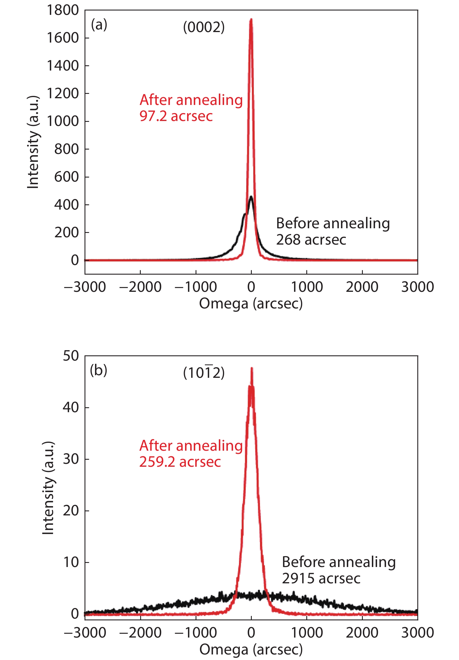
Fig. 1.
(Color online) The (a) (0002)- and (b) (10$ {\bar{1}} $![]()
![]()
2)-plane XRCs of the AlN films sputtered at 2000 W, 600 °C and 100 sccm N2 before and after HT annealing.
ARTICLES
Wen Gu1, 2, Zhibin Liu1, 2, 3, , Yanan Guo1, 2, 3, Xiaodong Wang1, 2, 3, Xiaolong Jia4, Xingfang Liu2, 5, Yiping Zeng4, 5, 6, Junxi Wang1, 2, 3, Jinmin Li1, 2, 3 and Jianchang Yan1, 2, 3,
Corresponding author: Zhibin Liu, E-mail: yanjc@semi.ac.cn and zbliu@semi.ac.cn; Jianchang Yan, E-mail: yanjc@semi.ac.cn and zbliu@semi.ac.cn
Abstract: High-quality AlN/sapphire templates were fabricated by the combination of sputtering and high-temperature (HT) annealing. The influence of sputtering parameters including nitrogen flux, radio frequency power, and substrate temperature on the crystalline quality and surface morphology of annealed AlN films were investigated. With lower substrate temperature, lower power, and lower N2 flux, the full width at half maximum of the X-ray rocking curve for AlN (0002) and (10
Key words: sputter, annealing, AlN, dislocation density
| [1] |
Li J M, Liu Z, Liu Z Q, et al. Advances and prospects in nitrides based light-emitting-diodes. J Semicond, 2016, 37, 061001 doi: 10.1088/1674-4926/37/6/061001
|
| [2] |
Wu Z H, Yan J C, Guo Y N, et al. Study of the morphology evolution of AlN grown on nano-patterned sapphire substrate. J Semicond, 2019, 40, 122803 doi: 10.1088/1674-4926/40/12/122803
|
| [3] |
Dong P, Yan J C, Zhang Y, et al. AlGaN-based deep ultraviolet light-emitting diodes grown on nano-patterned sapphire substrates with significant improvement in internal quantum efficiency. J Cryst Growth, 2014, 395, 9 doi: 10.1016/j.jcrysgro.2014.02.039
|
| [4] |
Ehrentraut D, Sitar Z. Advances in bulk crystal growth of AlN and GaN. MRS Bull, 2009, 34, 259 doi: 10.1557/mrs2009.76
|
| [5] |
Dalmau R, Moody B, Schlesser R, et al. Growth and characterization of AlN and AlGaN epitaxial films on AlN single crystal substrates. J Electrochem Soc, 2011, 158, H530 doi: 10.1149/1.3560527
|
| [6] |
Xu F J, Zhang L S, Xie N, et al. Realization of low dislocation density AlN on a small-coalescence-area nano-patterned sapphire substrate. CrystEngComm, 2019, 21, 2490 doi: 10.1039/C8CE01788C
|
| [7] |
Yan J C, Wang J X, Liu N X, et al. High quality AlGaN grown on a high temperature AIN template by MOCVD. J Semicond, 2009, 30, 103001 doi: 10.1088/1674-4926/30/10/103001
|
| [8] |
Yan J C, Wang J X, Zhang Y, et al. AlGaN-based deep-ultraviolet light-emitting diodes grown on High-quality AlN template using MOVPE. J Cryst Growth, 2015, 414, 254 doi: 10.1016/j.jcrysgro.2014.10.015
|
| [9] |
Chen X, Zhang Y, Yan J C, et al. Deep-ultraviolet stimulated emission from AlGaN/AlN multiple-quantum-wells on nano-patterned AlN/sapphire templates with reduced threshold power density. J Alloy Compd, 2017, 723, 192 doi: 10.1016/j.jallcom.2017.06.240
|
| [10] |
Dong P, Yan J C, Wang J X, et al. 282-nm AlGaN-based deep ultraviolet light-emitting diodes with improved performance on nano-patterned sapphire substrates. Appl Phys Lett, 2013, 102, 241113 doi: 10.1063/1.4812237
|
| [11] |
Chen X, Yan J C, Zhang Y, et al. Improved crystalline quality of AlN by epitaxial lateral overgrowth using two-phase growth method for deep-ultraviolet stimulated emission. IEEE Photonics J, 2016, 8, 1 doi: 10.1109/JPHOT.2016.2614102
|
| [12] |
Du Z J, Duan R F, Wei T B, et al. Producing deep UV-LEDs in high-yield MOVPE by improving AlN crystal quality with sputtered AlN nucleation layer. J Semicond, 2017, 38, 113003 doi: 10.1088/1674-4926/38/11/113003
|
| [13] |
Huang C, Wu P, Chang K, et al. High-quality and highly-transparent AlN template on annealed sputter-deposited AlN buffer layer for deep ultra-violet light-emitting diodes. AIP Adv, 2017, 7, 055110 doi: 10.1063/1.4983708
|
| [14] |
Susilo N, Hagedorn S, Jaeger D, et al. AlGaN-based deep UV LEDs grown on sputtered and high temperature annealed AlN/sapphire. Appl Phys Lett, 2018, 112, 041110 doi: 10.1063/1.5010265
|
| [15] |
Wang M X, Xu F J, Xie N, et al. Crystal quality evolution of AlN films via high-temperature annealing under ambient N2 conditions. CrystEngComm, 2018, 20, 6613 doi: 10.1039/C8CE00967H
|
| [16] |
Tanaka S, Shojiki K, Uesugi K, et al. Quantitative evaluation of strain relaxation in annealed sputter-deposited AlN film. J Cryst Growth, 2019, 512, 16 doi: 10.1016/j.jcrysgro.2019.02.001
|
| [17] |
Xiao S Y, Suzuki R, Miyake H, et al. Improvement mechanism of sputtered AlN films by high-temperature annealing. J Cryst Growth, 2018, 502, 41 doi: 10.1016/j.jcrysgro.2018.09.002
|
| [18] |
Kumada T, Ohtsuka M, Takada K, et al. Influence of sputter power and N2 gas flow ratio on crystalline quality of AlN layers deposited at 823 K by RF reactive sputtering. Phys Status Solidi C, 2012, 9, 515 doi: 10.1002/pssc.201100489
|
| [19] |
Miyake H, Lin C H, Tokoro K, et al. Preparation of high-quality AlN on sapphire by high-temperature face-to-face annealing. J Cryst Growth, 2016, 456, 155 doi: 10.1016/j.jcrysgro.2016.08.028
|
| [20] |
Fukuyama H, Miyake H, Nishio G, et al. Impact of high-temperature annealing of AlN layer on sapphire and its thermodynamic principle. Jpn J Appl Phys, 2016, 55, 05FL02 doi: 10.7567/JJAP.55.05FL02
|
| [21] |
Washiyama S, Guan Y, Mita S, et al. Recovery kinetics in high temperature annealed AlN heteroepitaxial films. J Appl Phys, 2020, 127, 115301 doi: 10.1063/5.0002891
|
| [22] |
Kumada T, Ohtsuka M, Fukuyama H. Influence of substrate temperature on the crystalline quality of AlN layers deposited by RF reactive magnetron sputtering. AIP Adv, 2015, 5, 017136 doi: 10.1063/1.4906796
|
| [23] |
Medjani F, Sanjinés R, Allidi G, et al. Effect of substrate temperature and bias voltage on the crystallite orientation in RF magnetron sputtered AlN thin films. Thin Solid Films, 2006, 515, 260 doi: 10.1016/j.tsf.2005.12.145
|
| [24] |
Yang S B, Miyagawa R, Miyake H, et al. Raman scattering spectroscopy of residual stresses in epitaxial AlN films. Appl Phys Express, 2011, 4, 031001 doi: 10.1143/APEX.4.031001
|
| [25] |
Guo Q X, Yahata K, Tanaka T, et al. Low-temperature growth of aluminum nitride on sapphire substrates. J Cryst Growth, 2003, 257, 123 doi: 10.1016/S0022-0248(03)01565-3
|
| [26] |
Zhao L, Yang K, Ai Y J, et al. Crystal quality improvement of sputtered AlN film on sapphire substrate by high-temperature annealing. J Mater Sci: Mater Electron, 2018, 29, 13766 doi: 10.1007/s10854-018-9507-0
|
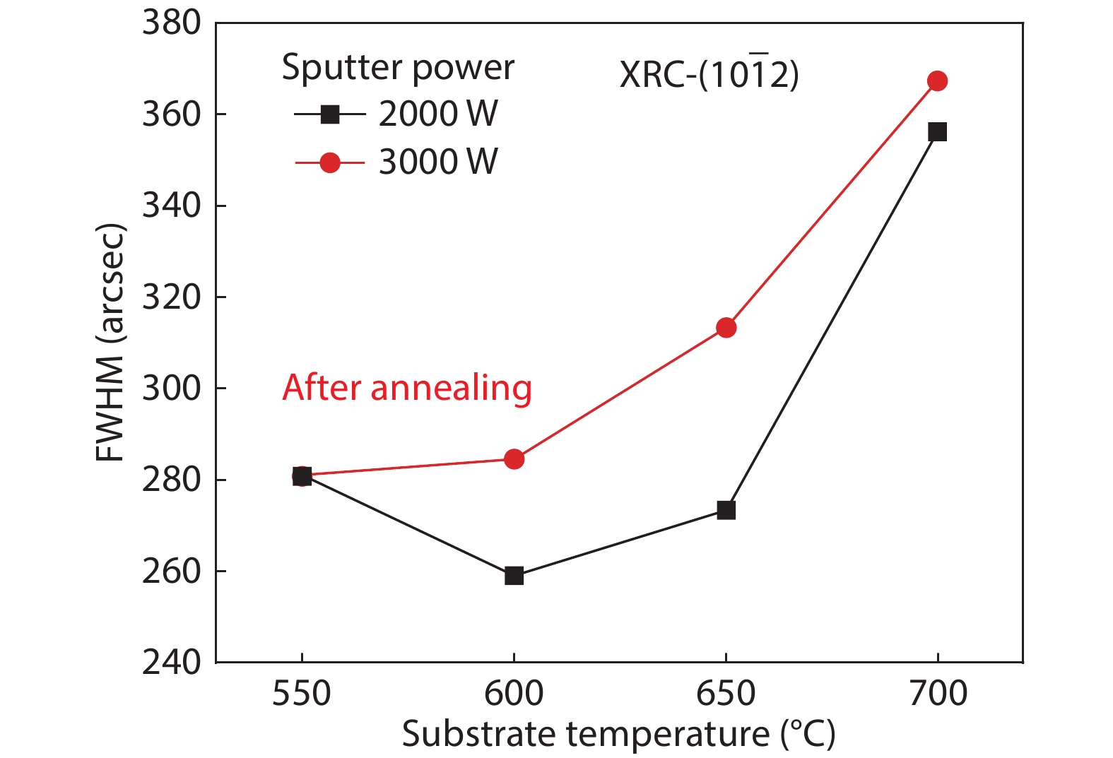
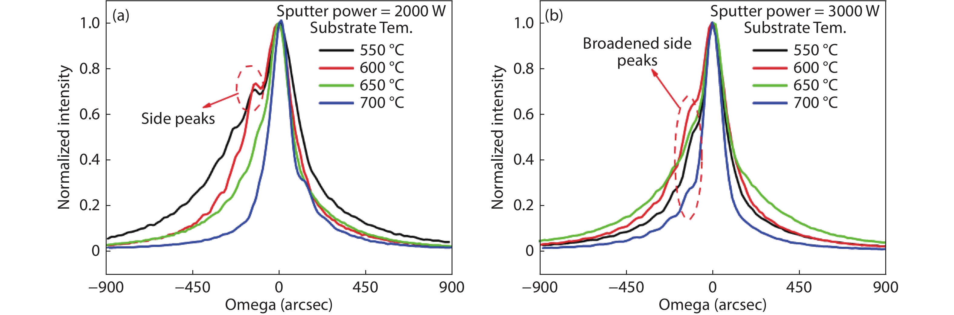
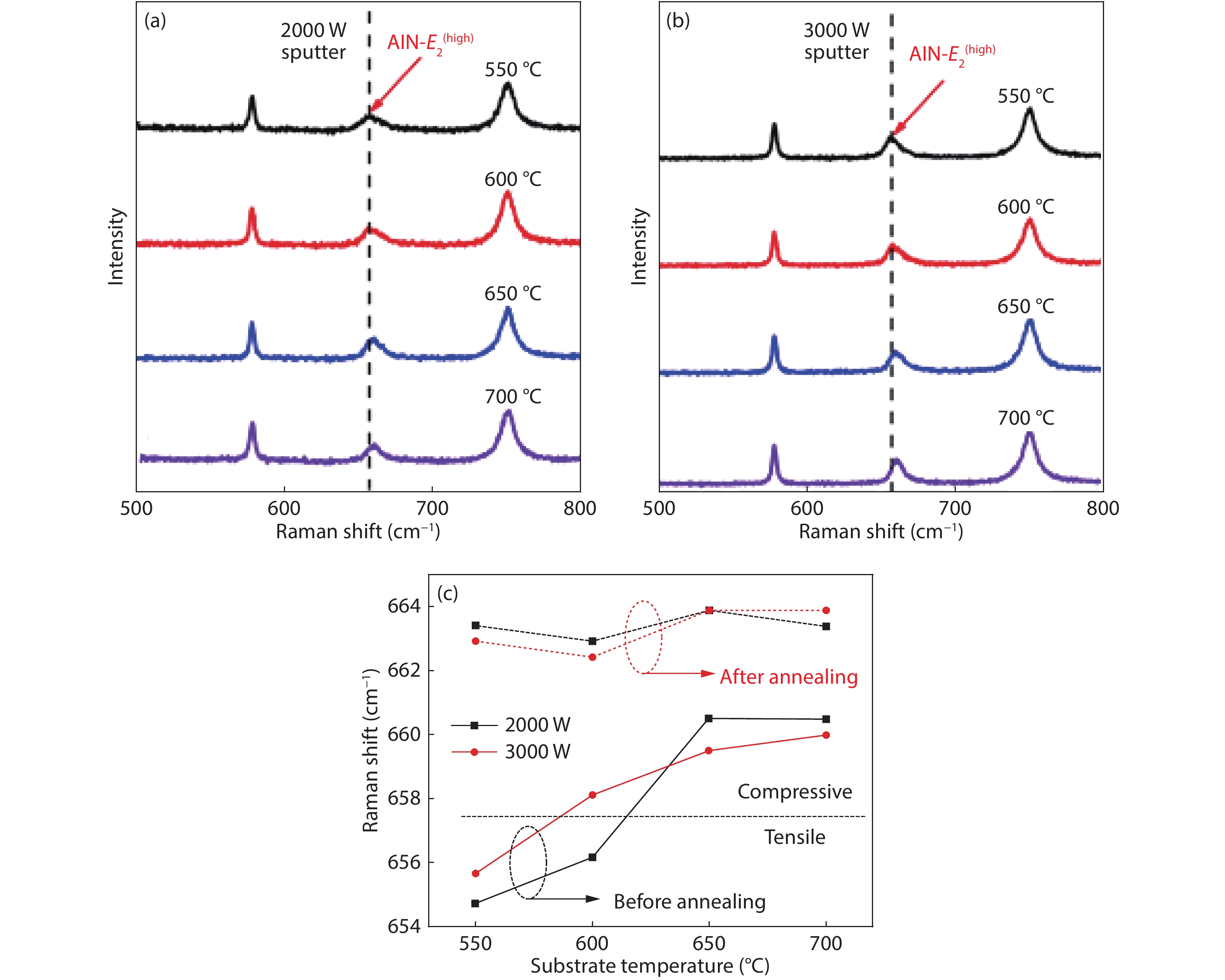
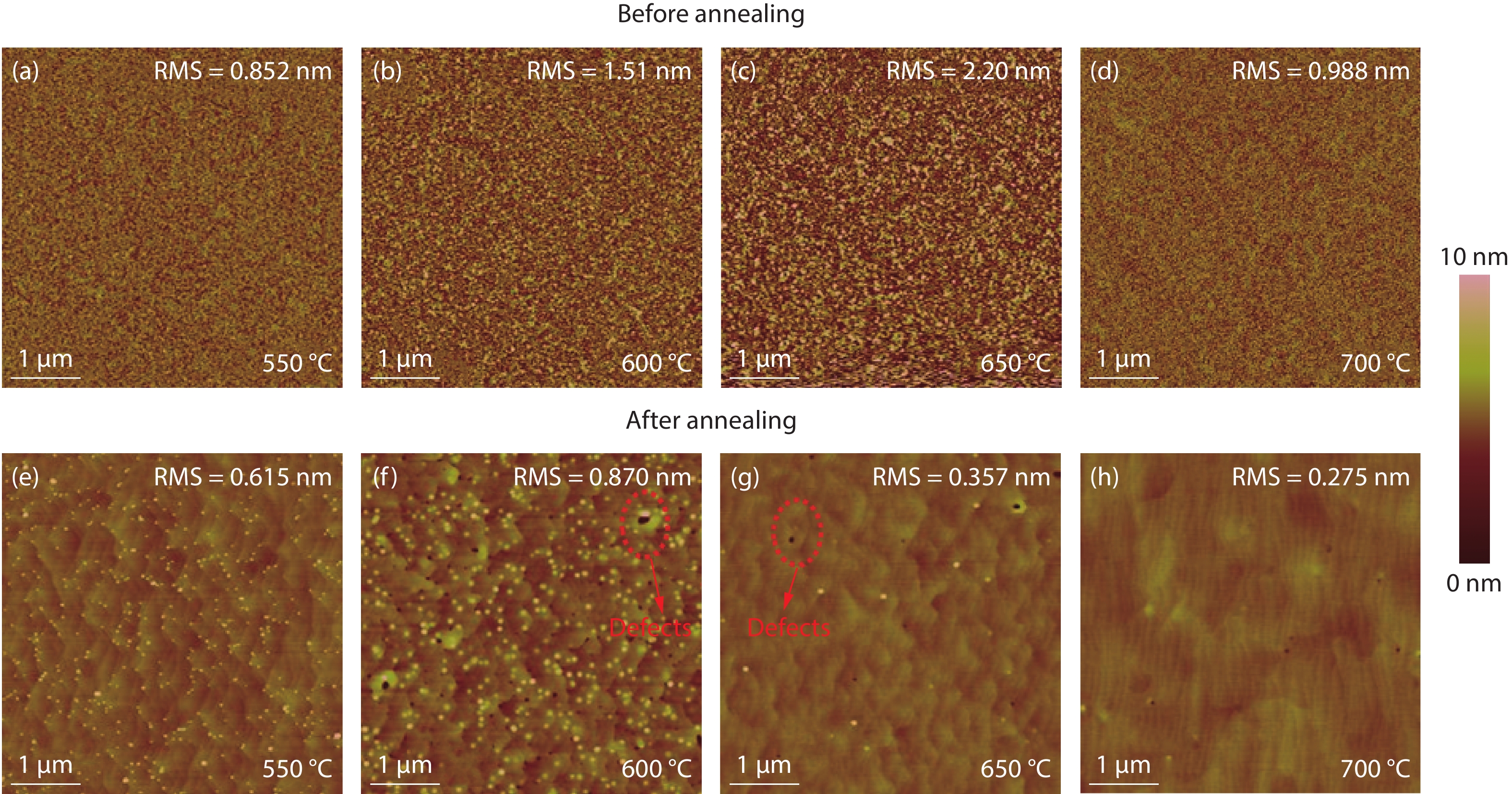
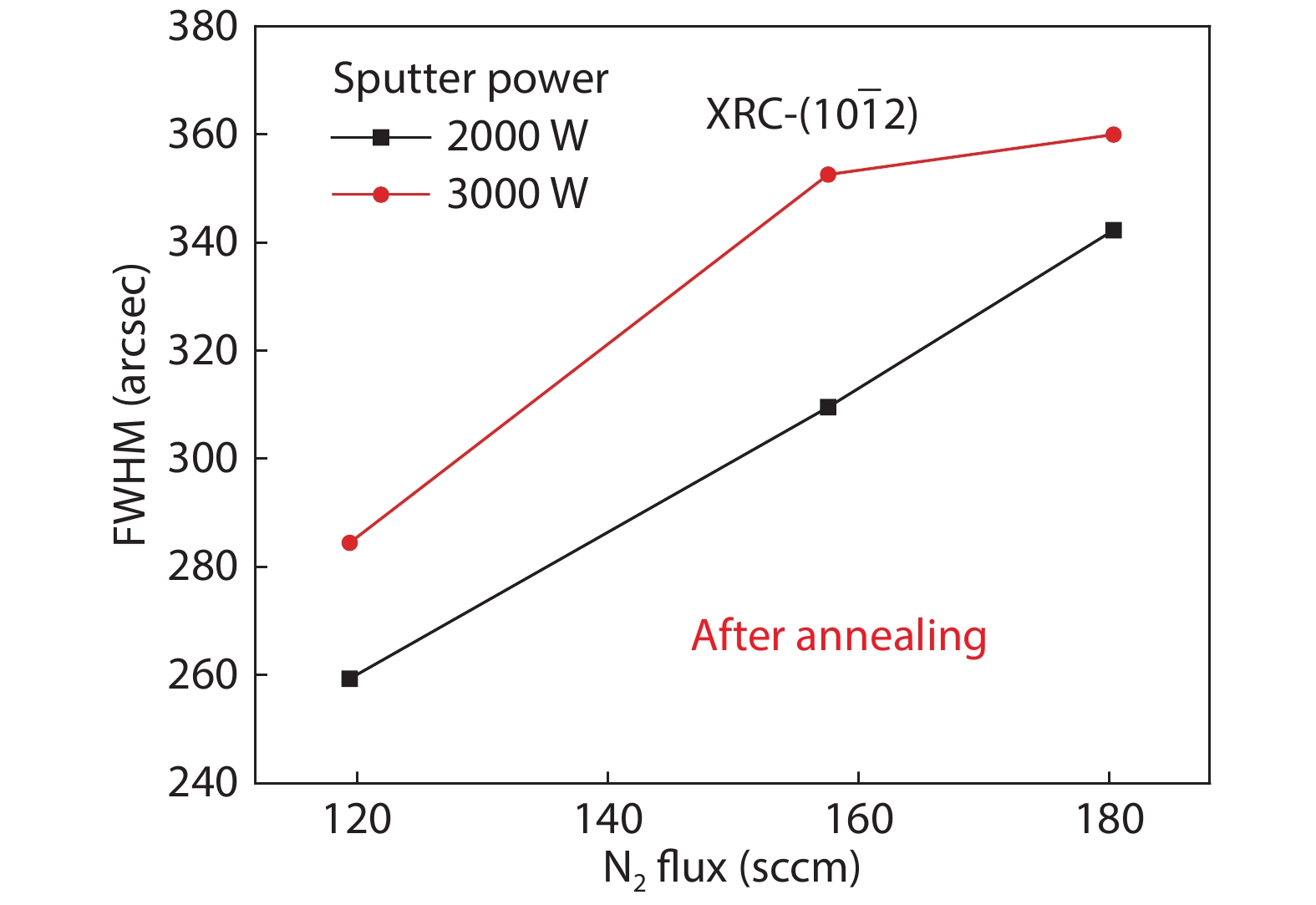
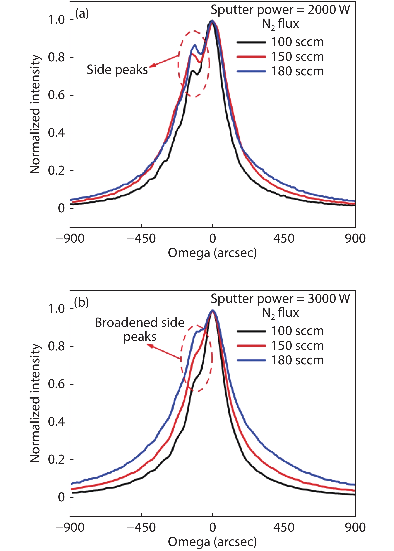

Table 1. Sputtering parameters for the deposition of AlN films.
| Sputtering parameter | Value |
| Target | Al (> 99.9999 at%) |
| Substrate | c-sapphire |
| Target to substrate distance | 64.8 mm |
| Substrate temperature | 550–700 °C |
| N2 flux | 100–190 sccm |
| RF power | 2000 and 3000 W |
| Process pressure | 0.31 to 0.55 Pa |
| Deposition rate | 0.20–0.32 nm/s |
| Targeted AlN thickness | 200 nm |
 DownLoad: CSV
Table 2. Characterizations for the sputtered AlN films.
| Sputtering condition | Deposition rate (nm/s) | Actual thickness (nm) | FWHM values of XRC (arcsec) | RMS (nm) | |
| (0002)-plane | (10 | ||||
| 2000 W, 100 sccm, 550 °C | 0.210 | 213.77 | 360 | 3229 | 0.852 |
| 2000 W, 100 sccm, 600 °C | 0.216 | 219.72 | 270 | 2941 | 1.510 |
| 2000 W, 100 sccm, 650 °C | 0.233 | 237.42 | 191 | 2714 | 2.200 |
| 2000 W, 100 sccm, 700 °C | 0.197 | 200.70 | 130 | 2491 | 0.988 |
| 3000 W, 100 sccm, 550 °C | 0.330 | 207.93 | 184 | 3301 | 0.850 |
| 3000 W, 100 sccm, 600 °C | 0.340 | 214.19 | 241 | 2923 | 0.995 |
| 3000 W, 100 sccm, 650 °C | 0.346 | 218.17 | 205 | 2664 | 1.060 |
| 3000 W, 100 sccm, 700 °C | 0.316 | 199.31 | 119 | 2584 | 0.955 |
| 2000 W, 150 sccm, 600 °C | 0.206 | 209.28 | 371 | 2776 | 1.860 |
| 2000 W, 180 sccm, 600 °C | 0.218 | 220.40 | 349 | 2743 | 1.930 |
| 3000 W, 150 sccm, 600 °C | 0.315 | 198.23 | 292 | 2966 | 1.970 |
| 3000 W, 180 sccm, 600 °C | 0.322 | 202.65 | 410 | 3049 | 2.010 |
DownLoad: CSV
| [1] |
Li J M, Liu Z, Liu Z Q, et al. Advances and prospects in nitrides based light-emitting-diodes. J Semicond, 2016, 37, 061001 doi: 10.1088/1674-4926/37/6/061001
|
| [2] |
Wu Z H, Yan J C, Guo Y N, et al. Study of the morphology evolution of AlN grown on nano-patterned sapphire substrate. J Semicond, 2019, 40, 122803 doi: 10.1088/1674-4926/40/12/122803
|
| [3] |
Dong P, Yan J C, Zhang Y, et al. AlGaN-based deep ultraviolet light-emitting diodes grown on nano-patterned sapphire substrates with significant improvement in internal quantum efficiency. J Cryst Growth, 2014, 395, 9 doi: 10.1016/j.jcrysgro.2014.02.039
|
| [4] |
Ehrentraut D, Sitar Z. Advances in bulk crystal growth of AlN and GaN. MRS Bull, 2009, 34, 259 doi: 10.1557/mrs2009.76
|
| [5] |
Dalmau R, Moody B, Schlesser R, et al. Growth and characterization of AlN and AlGaN epitaxial films on AlN single crystal substrates. J Electrochem Soc, 2011, 158, H530 doi: 10.1149/1.3560527
|
| [6] |
Xu F J, Zhang L S, Xie N, et al. Realization of low dislocation density AlN on a small-coalescence-area nano-patterned sapphire substrate. CrystEngComm, 2019, 21, 2490 doi: 10.1039/C8CE01788C
|
| [7] |
Yan J C, Wang J X, Liu N X, et al. High quality AlGaN grown on a high temperature AIN template by MOCVD. J Semicond, 2009, 30, 103001 doi: 10.1088/1674-4926/30/10/103001
|
| [8] |
Yan J C, Wang J X, Zhang Y, et al. AlGaN-based deep-ultraviolet light-emitting diodes grown on High-quality AlN template using MOVPE. J Cryst Growth, 2015, 414, 254 doi: 10.1016/j.jcrysgro.2014.10.015
|
| [9] |
Chen X, Zhang Y, Yan J C, et al. Deep-ultraviolet stimulated emission from AlGaN/AlN multiple-quantum-wells on nano-patterned AlN/sapphire templates with reduced threshold power density. J Alloy Compd, 2017, 723, 192 doi: 10.1016/j.jallcom.2017.06.240
|
| [10] |
Dong P, Yan J C, Wang J X, et al. 282-nm AlGaN-based deep ultraviolet light-emitting diodes with improved performance on nano-patterned sapphire substrates. Appl Phys Lett, 2013, 102, 241113 doi: 10.1063/1.4812237
|
| [11] |
Chen X, Yan J C, Zhang Y, et al. Improved crystalline quality of AlN by epitaxial lateral overgrowth using two-phase growth method for deep-ultraviolet stimulated emission. IEEE Photonics J, 2016, 8, 1 doi: 10.1109/JPHOT.2016.2614102
|
| [12] |
Du Z J, Duan R F, Wei T B, et al. Producing deep UV-LEDs in high-yield MOVPE by improving AlN crystal quality with sputtered AlN nucleation layer. J Semicond, 2017, 38, 113003 doi: 10.1088/1674-4926/38/11/113003
|
| [13] |
Huang C, Wu P, Chang K, et al. High-quality and highly-transparent AlN template on annealed sputter-deposited AlN buffer layer for deep ultra-violet light-emitting diodes. AIP Adv, 2017, 7, 055110 doi: 10.1063/1.4983708
|
| [14] |
Susilo N, Hagedorn S, Jaeger D, et al. AlGaN-based deep UV LEDs grown on sputtered and high temperature annealed AlN/sapphire. Appl Phys Lett, 2018, 112, 041110 doi: 10.1063/1.5010265
|
| [15] |
Wang M X, Xu F J, Xie N, et al. Crystal quality evolution of AlN films via high-temperature annealing under ambient N2 conditions. CrystEngComm, 2018, 20, 6613 doi: 10.1039/C8CE00967H
|
| [16] |
Tanaka S, Shojiki K, Uesugi K, et al. Quantitative evaluation of strain relaxation in annealed sputter-deposited AlN film. J Cryst Growth, 2019, 512, 16 doi: 10.1016/j.jcrysgro.2019.02.001
|
| [17] |
Xiao S Y, Suzuki R, Miyake H, et al. Improvement mechanism of sputtered AlN films by high-temperature annealing. J Cryst Growth, 2018, 502, 41 doi: 10.1016/j.jcrysgro.2018.09.002
|
| [18] |
Kumada T, Ohtsuka M, Takada K, et al. Influence of sputter power and N2 gas flow ratio on crystalline quality of AlN layers deposited at 823 K by RF reactive sputtering. Phys Status Solidi C, 2012, 9, 515 doi: 10.1002/pssc.201100489
|
| [19] |
Miyake H, Lin C H, Tokoro K, et al. Preparation of high-quality AlN on sapphire by high-temperature face-to-face annealing. J Cryst Growth, 2016, 456, 155 doi: 10.1016/j.jcrysgro.2016.08.028
|
| [20] |
Fukuyama H, Miyake H, Nishio G, et al. Impact of high-temperature annealing of AlN layer on sapphire and its thermodynamic principle. Jpn J Appl Phys, 2016, 55, 05FL02 doi: 10.7567/JJAP.55.05FL02
|
| [21] |
Washiyama S, Guan Y, Mita S, et al. Recovery kinetics in high temperature annealed AlN heteroepitaxial films. J Appl Phys, 2020, 127, 115301 doi: 10.1063/5.0002891
|
| [22] |
Kumada T, Ohtsuka M, Fukuyama H. Influence of substrate temperature on the crystalline quality of AlN layers deposited by RF reactive magnetron sputtering. AIP Adv, 2015, 5, 017136 doi: 10.1063/1.4906796
|
| [23] |
Medjani F, Sanjinés R, Allidi G, et al. Effect of substrate temperature and bias voltage on the crystallite orientation in RF magnetron sputtered AlN thin films. Thin Solid Films, 2006, 515, 260 doi: 10.1016/j.tsf.2005.12.145
|
| [24] |
Yang S B, Miyagawa R, Miyake H, et al. Raman scattering spectroscopy of residual stresses in epitaxial AlN films. Appl Phys Express, 2011, 4, 031001 doi: 10.1143/APEX.4.031001
|
| [25] |
Guo Q X, Yahata K, Tanaka T, et al. Low-temperature growth of aluminum nitride on sapphire substrates. J Cryst Growth, 2003, 257, 123 doi: 10.1016/S0022-0248(03)01565-3
|
| [26] |
Zhao L, Yang K, Ai Y J, et al. Crystal quality improvement of sputtered AlN film on sapphire substrate by high-temperature annealing. J Mater Sci: Mater Electron, 2018, 29, 13766 doi: 10.1007/s10854-018-9507-0
|


Article views: 5644 Times PDF downloads: 171 Times Cited by: 0 Times
Received: 29 March 2020 Revised: 08 May 2020 Online: Accepted Manuscript: 03 August 2020Uncorrected proof: 10 August 2020Published: 08 December 2020
| Citation: |
Wen Gu, Zhibin Liu, Yanan Guo, Xiaodong Wang, Xiaolong Jia, Xingfang Liu, Yiping Zeng, Junxi Wang, Jinmin Li, Jianchang Yan. Comprehensive study of crystalline AlN/sapphire templates after high-temperature annealing with various sputtering conditions[J]. Journal of Semiconductors, 2020, 41(12): 122802. doi: 10.1088/1674-4926/41/12/122802
****
W Gu, Z B Liu, Y N Guo, X D Wang, X L Jia, X F Liu, Y P Zeng, J X Wang, J M Li, J C Yan, Comprehensive study of crystalline AlN/sapphire templates after high-temperature annealing with various sputtering conditions[J]. J. Semicond., 2020, 41(12): 122802. doi: 10.1088/1674-4926/41/12/122802.

|
| [1] |
Li J M, Liu Z, Liu Z Q, et al. Advances and prospects in nitrides based light-emitting-diodes. J Semicond, 2016, 37, 061001 doi: 10.1088/1674-4926/37/6/061001
|
| [2] |
Wu Z H, Yan J C, Guo Y N, et al. Study of the morphology evolution of AlN grown on nano-patterned sapphire substrate. J Semicond, 2019, 40, 122803 doi: 10.1088/1674-4926/40/12/122803
|
| [3] |
Dong P, Yan J C, Zhang Y, et al. AlGaN-based deep ultraviolet light-emitting diodes grown on nano-patterned sapphire substrates with significant improvement in internal quantum efficiency. J Cryst Growth, 2014, 395, 9 doi: 10.1016/j.jcrysgro.2014.02.039
|
| [4] |
Ehrentraut D, Sitar Z. Advances in bulk crystal growth of AlN and GaN. MRS Bull, 2009, 34, 259 doi: 10.1557/mrs2009.76
|
| [5] |
Dalmau R, Moody B, Schlesser R, et al. Growth and characterization of AlN and AlGaN epitaxial films on AlN single crystal substrates. J Electrochem Soc, 2011, 158, H530 doi: 10.1149/1.3560527
|
| [6] |
Xu F J, Zhang L S, Xie N, et al. Realization of low dislocation density AlN on a small-coalescence-area nano-patterned sapphire substrate. CrystEngComm, 2019, 21, 2490 doi: 10.1039/C8CE01788C
|
| [7] |
Yan J C, Wang J X, Liu N X, et al. High quality AlGaN grown on a high temperature AIN template by MOCVD. J Semicond, 2009, 30, 103001 doi: 10.1088/1674-4926/30/10/103001
|
| [8] |
Yan J C, Wang J X, Zhang Y, et al. AlGaN-based deep-ultraviolet light-emitting diodes grown on High-quality AlN template using MOVPE. J Cryst Growth, 2015, 414, 254 doi: 10.1016/j.jcrysgro.2014.10.015
|
| [9] |
Chen X, Zhang Y, Yan J C, et al. Deep-ultraviolet stimulated emission from AlGaN/AlN multiple-quantum-wells on nano-patterned AlN/sapphire templates with reduced threshold power density. J Alloy Compd, 2017, 723, 192 doi: 10.1016/j.jallcom.2017.06.240
|
| [10] |
Dong P, Yan J C, Wang J X, et al. 282-nm AlGaN-based deep ultraviolet light-emitting diodes with improved performance on nano-patterned sapphire substrates. Appl Phys Lett, 2013, 102, 241113 doi: 10.1063/1.4812237
|
| [11] |
Chen X, Yan J C, Zhang Y, et al. Improved crystalline quality of AlN by epitaxial lateral overgrowth using two-phase growth method for deep-ultraviolet stimulated emission. IEEE Photonics J, 2016, 8, 1 doi: 10.1109/JPHOT.2016.2614102
|
| [12] |
Du Z J, Duan R F, Wei T B, et al. Producing deep UV-LEDs in high-yield MOVPE by improving AlN crystal quality with sputtered AlN nucleation layer. J Semicond, 2017, 38, 113003 doi: 10.1088/1674-4926/38/11/113003
|
| [13] |
Huang C, Wu P, Chang K, et al. High-quality and highly-transparent AlN template on annealed sputter-deposited AlN buffer layer for deep ultra-violet light-emitting diodes. AIP Adv, 2017, 7, 055110 doi: 10.1063/1.4983708
|
| [14] |
Susilo N, Hagedorn S, Jaeger D, et al. AlGaN-based deep UV LEDs grown on sputtered and high temperature annealed AlN/sapphire. Appl Phys Lett, 2018, 112, 041110 doi: 10.1063/1.5010265
|
| [15] |
Wang M X, Xu F J, Xie N, et al. Crystal quality evolution of AlN films via high-temperature annealing under ambient N2 conditions. CrystEngComm, 2018, 20, 6613 doi: 10.1039/C8CE00967H
|
| [16] |
Tanaka S, Shojiki K, Uesugi K, et al. Quantitative evaluation of strain relaxation in annealed sputter-deposited AlN film. J Cryst Growth, 2019, 512, 16 doi: 10.1016/j.jcrysgro.2019.02.001
|
| [17] |
Xiao S Y, Suzuki R, Miyake H, et al. Improvement mechanism of sputtered AlN films by high-temperature annealing. J Cryst Growth, 2018, 502, 41 doi: 10.1016/j.jcrysgro.2018.09.002
|
| [18] |
Kumada T, Ohtsuka M, Takada K, et al. Influence of sputter power and N2 gas flow ratio on crystalline quality of AlN layers deposited at 823 K by RF reactive sputtering. Phys Status Solidi C, 2012, 9, 515 doi: 10.1002/pssc.201100489
|
| [19] |
Miyake H, Lin C H, Tokoro K, et al. Preparation of high-quality AlN on sapphire by high-temperature face-to-face annealing. J Cryst Growth, 2016, 456, 155 doi: 10.1016/j.jcrysgro.2016.08.028
|
| [20] |
Fukuyama H, Miyake H, Nishio G, et al. Impact of high-temperature annealing of AlN layer on sapphire and its thermodynamic principle. Jpn J Appl Phys, 2016, 55, 05FL02 doi: 10.7567/JJAP.55.05FL02
|
| [21] |
Washiyama S, Guan Y, Mita S, et al. Recovery kinetics in high temperature annealed AlN heteroepitaxial films. J Appl Phys, 2020, 127, 115301 doi: 10.1063/5.0002891
|
| [22] |
Kumada T, Ohtsuka M, Fukuyama H. Influence of substrate temperature on the crystalline quality of AlN layers deposited by RF reactive magnetron sputtering. AIP Adv, 2015, 5, 017136 doi: 10.1063/1.4906796
|
| [23] |
Medjani F, Sanjinés R, Allidi G, et al. Effect of substrate temperature and bias voltage on the crystallite orientation in RF magnetron sputtered AlN thin films. Thin Solid Films, 2006, 515, 260 doi: 10.1016/j.tsf.2005.12.145
|
| [24] |
Yang S B, Miyagawa R, Miyake H, et al. Raman scattering spectroscopy of residual stresses in epitaxial AlN films. Appl Phys Express, 2011, 4, 031001 doi: 10.1143/APEX.4.031001
|
| [25] |
Guo Q X, Yahata K, Tanaka T, et al. Low-temperature growth of aluminum nitride on sapphire substrates. J Cryst Growth, 2003, 257, 123 doi: 10.1016/S0022-0248(03)01565-3
|
| [26] |
Zhao L, Yang K, Ai Y J, et al. Crystal quality improvement of sputtered AlN film on sapphire substrate by high-temperature annealing. J Mater Sci: Mater Electron, 2018, 29, 13766 doi: 10.1007/s10854-018-9507-0
|

 WeChat ID
Journal of Semiconductors © 2017 All Rights Reserved 京ICP備05085259號-2

