


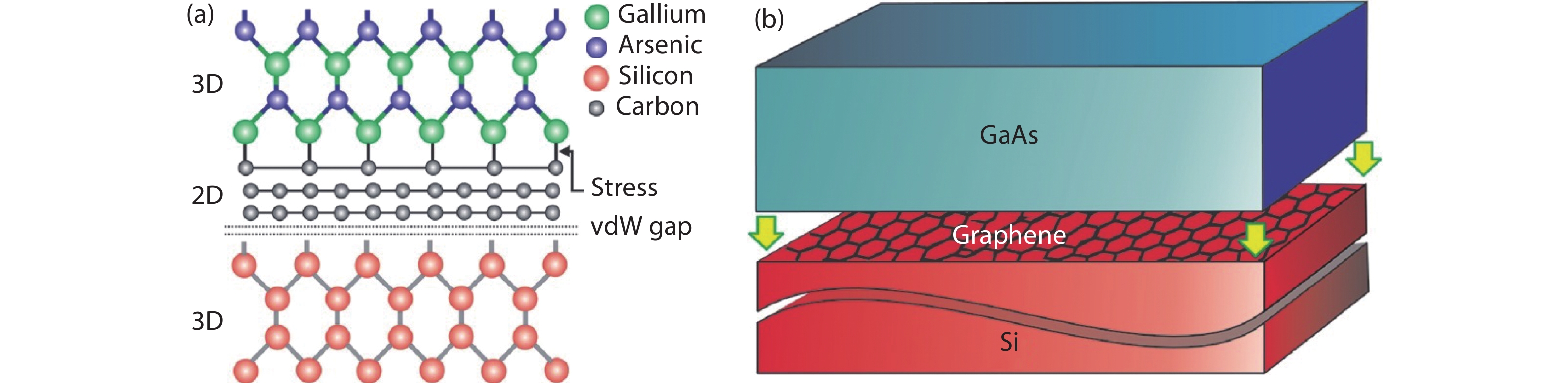
Fig. 1.
(Color online) (a) Schematic atomic geometry and (b) schematic epitaxial structure of GaAs thin film on graphene-coated Si substrate[3].
NEWS AND VIEWS
Corresponding author: Yi Gu, guyi@mail.sitp.ac.cn
| [1] |
Chung K, Lee C H, Yi G C. Transferable GaN layers grown on ZnO-coated graphene layers for optoelectronic devices. Science, 2010, 330, 655 doi: 10.1126/science.1195403
|
| [2] |
Kim J, Bayram C, Park H, et al. Principle of direct van der Waals epitaxy of single-crystalline films on epitaxial graphene. Nat Commun, 2014, 5, 4836 doi: 10.1038/ncomms5836
|
| [3] |
Alaskar Y, Arafin S, Wickramaratne D, et al. Towards van der Waals epitaxial growth of GaAs on Si using a graphene buffer layer. Adv Funct Mater, 2014, 24, 6629 doi: 10.1002/adfm.v24.42
|
| [4] |
Kim Y, Cruz S, Lee K, et al. Remote epitaxy through graphene enables two-dimensional material-based layer transfer. Nature, 2017, 544, 340 doi: 10.1038/nature22053
|
| [5] |
Kong W, Li H, Qiao K, et al. Polarity governs atomic interaction through two-dimensional materials. Nat Mater, 2018, 17, 999 doi: 10.1038/s41563-018-0176-4
|


Article views: 5428 Times PDF downloads: 108 Times Cited by: 0 Times
Received: Revised: Online: Accepted Manuscript: 04 April 2019Uncorrected proof: 31 May 2019Published: 05 June 2019
| Citation: |
Yi Gu. Heteroepitaxy of semiconductor thin films[J]. Journal of Semiconductors, 2019, 40(6): 060401. doi: 10.1088/1674-4926/40/6/060401
****
Y Gu, Heteroepitaxy of semiconductor thin films[J]. J. Semicond., 2019, 40(6): 060401. doi: 10.1088/1674-4926/40/6/060401.

|
| [1] |
Chung K, Lee C H, Yi G C. Transferable GaN layers grown on ZnO-coated graphene layers for optoelectronic devices. Science, 2010, 330, 655 doi: 10.1126/science.1195403
|
| [2] |
Kim J, Bayram C, Park H, et al. Principle of direct van der Waals epitaxy of single-crystalline films on epitaxial graphene. Nat Commun, 2014, 5, 4836 doi: 10.1038/ncomms5836
|
| [3] |
Alaskar Y, Arafin S, Wickramaratne D, et al. Towards van der Waals epitaxial growth of GaAs on Si using a graphene buffer layer. Adv Funct Mater, 2014, 24, 6629 doi: 10.1002/adfm.v24.42
|
| [4] |
Kim Y, Cruz S, Lee K, et al. Remote epitaxy through graphene enables two-dimensional material-based layer transfer. Nature, 2017, 544, 340 doi: 10.1038/nature22053
|
| [5] |
Kong W, Li H, Qiao K, et al. Polarity governs atomic interaction through two-dimensional materials. Nat Mater, 2018, 17, 999 doi: 10.1038/s41563-018-0176-4
|

 WeChat ID
Journal of Semiconductors © 2017 All Rights Reserved 京ICP備05085259號-2
 DownLoad:

