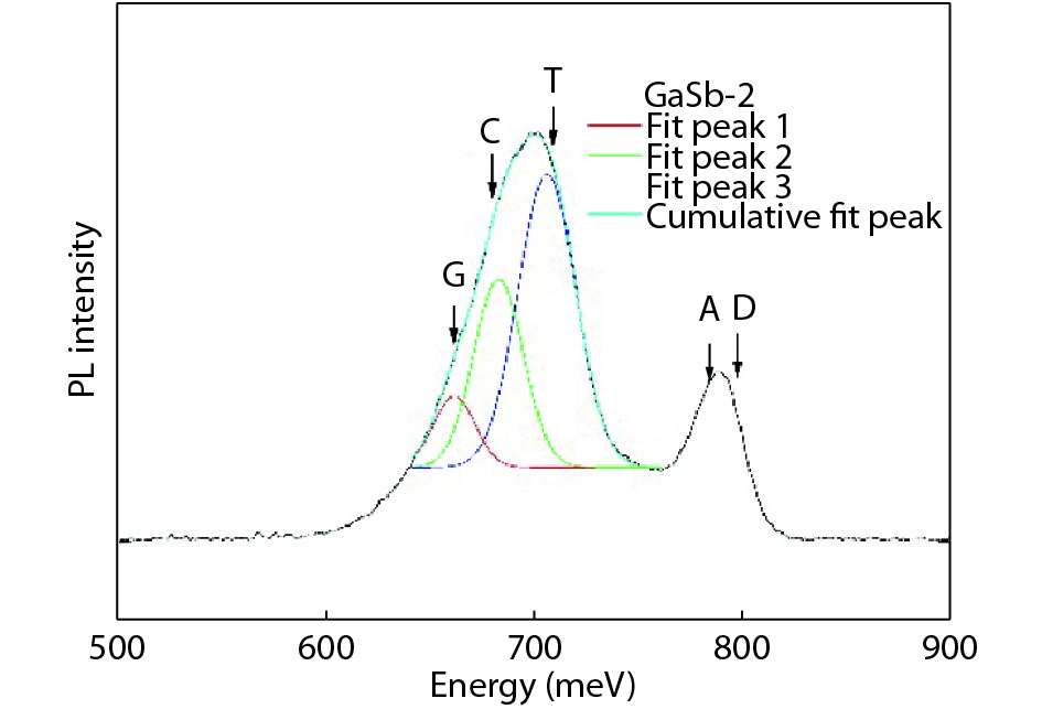
Fig. 2.
(Color online) PL spectra of sample 2 at 10 K.
ARTICLES
Guiying Shen1, Youwen Zhao1, 2, Yongbiao Bai1, , Jingming Liu1, Hui Xie1, Zhiyuan Dong1, Jun Yang1 and Ding Yu1, 2
Corresponding author: Yongbiao Bai, baiyongbiao@semi.ac.cn
Abstract: Lightly Te-doped GaSb samples grown by the liquid encapsulated Czochralski (LEC) method have been studied by Hall measurements and low-temperature PL spectroscopy. The results suggest that acceptor-related antisite is the dominant defect in n-type GaSb with low Te-doping concentration. As the Te concentration increases, gallium vacancy related defects become the main acceptor. A new band of around 665 meV is observed in the GaSb sample with the lowest Te-doping concentration. The variation of the acceptor defects and their influence on the electronic and optical property on the n-GaSb single crystal are discussed based on the results.
Key words: Te-doped GaSb, Hall, native defects, PL
| [1] |
Dutta P S, Bhat H L, Kumar V. The physics and technology of gallium antimonide: An emerging optoelectronic material. J Appl Phys, 1997, 81, 5821 doi: 10.1063/1.365356
|
| [2] |
Zia N, Viheri?l? J, Koskinen R, et al. High power (60 mW) GaSb-based 1.9 μm superluminescent diode with cavity suppression element. Appl Phys Lett, 2016, 109, 231102 doi: 10.1063/1.4971972
|
| [3] |
Zhou X, Li D, Huang J, et al. Mid-wavelength type II InAs/GaSb superlattice infrared focal plane arrays. Infrared Phys Technol, 2016, 78, 263 doi: 10.1016/j.infrared.2016.08.014
|
| [4] |
Haugan H J, Brown G J, Szmulowicz F, et al. InAs/GaSb type-II superlattices for high performance mid-infrared detectors. J Cryst Growth, 2005, 278, 198 doi: 10.1016/j.jcrysgro.2005.01.006
|
| [5] |
Su J, Liu T, Liu J M, et al. Thermally induced native defect transform in annealed GaSb. Chin Phys B, 2016, 25, 077801 doi: 10.1088/1674-1056/25/7/077801
|
| [6] |
Kujala J, Segercrantz N, Tuomisto F, et al. Native point defects in GaSb. J Appl Phys, 2014, 116, 143508 doi: 10.1063/1.4898082
|
| [7] |
Segercrantz N, Slotte J, Makkonen I, et al. Point defect balance in epitaxial GaSb. Appl Phys Lett, 2014, 105, 082113 doi: 10.1063/1.4894473
|
| [8] |
Tahini H A, Chroneos A, Murphy S T, et al. Vacancies and defect levels in III–V semiconductors. J Appl Phys, 2013, 114, 063517 doi: 10.1063/1.4818484
|
| [9] |
Vlasov A S, Rakova E P, Khvostikov V P, et al. Native defect concentration in Czochralski-grown Te-doped GaSb by photoluminescence. Sol Energ Mat Sol C, 2010, 94, 1113 doi: 10.1016/j.solmat.2010.02.038
|
| [10] |
Hu W G, Wang Z, Su B F, et al. Gallium antisite defect and residual acceptors in undoped GaSb. Phys Lett A, 2004, 332, 286 doi: 10.1016/j.physleta.2004.09.056
|
| [11] |
Rudolph P, Czupalla M, Lux B. LEC growth of semi-insulating GaAs crystals in traveling magnetic field generated in a heater–magnet module. J Cryst Growth, 2009, 311, 4543 doi: 10.1016/j.jcrysgro.2009.08.024
|
| [12] |
Houchens B C, Becla P, Tritchler S E, et al. Crystal growth of bulk ternary semiconductors: comparison of GaInSb growth by horizontal Bridgman and horizontal traveling heater method. J Cryst Growth, 2010, 312, 1091 doi: 10.1016/j.jcrysgro.2009.12.051
|
| [13] |
Mo P G, Tan H Z, Du L X, et al. A novel technique for Czochralski growth of GaSb single crystals. J Cryst Growth, 1993, 126, 613 doi: 10.1016/0022-0248(93)90811-A
|
| [14] |
Pino R, Ko Y, Dutta P S. Enhancement of infrared transmission in GaSb bulk crystals by carrier compensation. J Appl Phys, 2004, 96, 1064 doi: 10.1063/1.1738527
|
| [15] |
Bai Y B, Zhao Y W, Shen G Y, et al. N-type GaSb single crystals with high below-band gap transmission. Chin Phys B, 2017, 26, 107801 doi: 10.1088/1674-1056/26/10/107801
|
| [16] |
Chandola A, Pino R, Dutta P S. Below bandgap optical absorption in tellurium-doped GaSb. Semicond Sci Technol, 2005, 20, 886 doi: 10.1088/0268-1242/20/8/046
|
| [17] |
Bignazzi A, Bosacchi A, Magnanini R. Photoluminescence study of heavy doping effects in Te-doped GaSb. J Appl Phys, 1997, 81, 7540 doi: 10.1063/1.365297
|
| [18] |
Wu M C, Chen C C. Photoluminescence of liquid-phase epitaxial Te-doped GaSb. J Appl Phys, 1993, 73, 8495 doi: 10.1063/1.354085
|
| [19] |
Dutta P S, Rao K S R K, Bhat H L, et al. Photoluminescence studies in bulk gallium antimonide. Appl Phys A, 1995, 61, 149 doi: 10.1007/BF01538381
|
| [20] |
Jiang W J, Sun Y M, Wu M C. Electrical and photoluminescent properties of high-quality GaSb and AlGaSb layers grown from Sb-rich solutions by liquid-phase epitaxy. J Appl Phys, 1995, 77, 1725 doi: 10.1063/1.359576
|
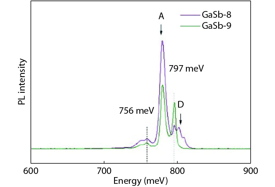
Table 1. Hall results of n-type Te-GaSb sample at room temperature.
| Sample No. | Mobility (cm2/(V·s)) | Carrier concentration (cm?3) | Type |
| 1 | 2.34 × 10³ | 1.66 × 10¹⁶ | n |
| 2 | 2.83 × 10³ | 2.79 × 10¹⁶ | n |
| 3 | 2.94 × 10³ | 5.24 × 10¹⁶ | n |
| 4 | 2.96 × 10³ | 6.63 × 10¹⁶ | n |
| 5 | 3.04 × 10³ | 7.84 × 10¹⁶ | n |
| 6 | 3.34 × 10³ | 1.14 × 10¹⁷ | n |
| 7 | 3.24 × 10³ | 1.38 × 10¹⁷ | n |
| 8 | 6.41 × 10² | 1.41 × 10¹⁷ | p |
| 9 | 7.39 × 10² | 1.14 × 10¹⁷ | p |
 DownLoad: CSV
Table 2. The PL peak position and related transition of GaSb reported in the literature.
| Energy (meV) | Transition | Quota |
| 812 | Band gap | Ref. [19] (4.2 K) |
| 810 | Free exciton | Ref. [20] (20 K) |
| 808 | Excitonic transition | Ref. [18] (19 K) |
| 802 | Donor-acceptor transition | Ref. [19] (4.2 K) |
| 797 | Excitonic transition | Ref. [18] (19 K) |
| 796, 792 | Exciton band to (VGa GaSb)0 | Ref. [19] (4.2 K) |
| 781 | C-(VGa GaSb)0 | Ref. [19] (4.2 K) |
| 777 | D+-(VGa GaSb)0 | Ref. [19] (4.2 K) |
| 765 | LO phonon replica of 796 meV transition | Ref. [18] (19 K) |
| 760 | Acceptor B | Ref. [18] (19 K) |
| 756 | Exciton band to GaSb | Ref. [5] (10 K) |
| 746, 740 | LO phonon replica of 777 meV | Ref. [19] (4.2 K) |
| 738 | C-(VGa GaSb TeSb ) | Ref. [18] (19 K) |
| 710 | C-(VGa GaSb) | Ref. [19] (4.2 K) |
| 682 | LO phonon replica of 710 meV | Ref. [19] (4.2 K) |
DownLoad: CSV
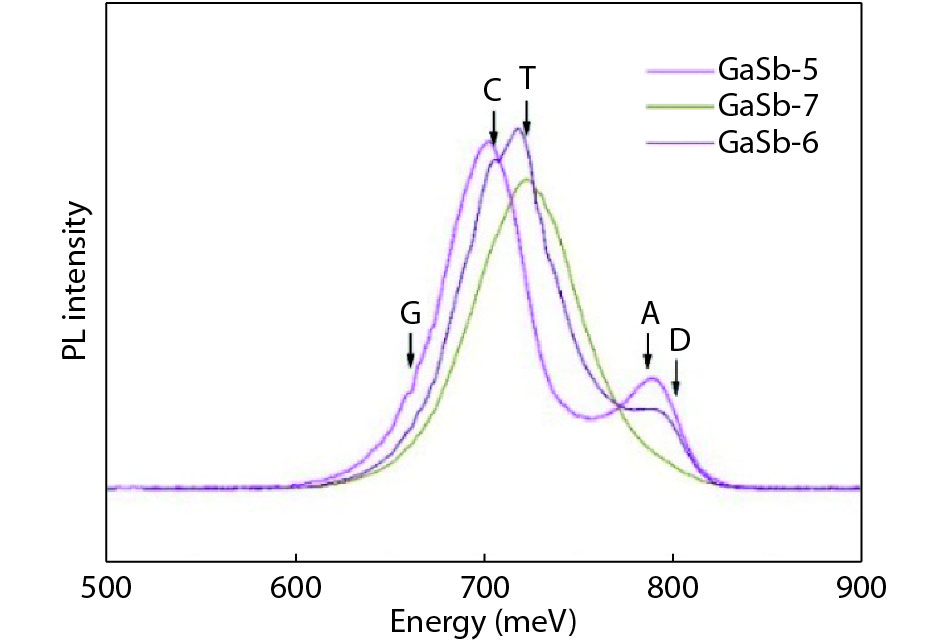
Table 3. The position (meV) and intensity (a.u.) of resolved peak G, C and T.
| Sample No. | Peak position | Strength of peak G | Peak position | Strength of peak C | Peak position | Strength of peak T |
| 1 | 665 | 0.65 | 683 | 1.26 | 703 | 1.73 |
| 2 | 664 | 0.52 | 683 | 1.43 | 706 | 1.68 |
| 3 | 664 | 0.43 | 685 | 1.52 | 708 | 1.53 |
| 4 | 665 | 0.42 | 686 | 1.58 | 707 | 1.56 |
| 5 | 666 | 0.12 | 692 | 0.92 | 712 | 1.59 |
| 6 | – | – | 700 | 0.83 | 721 | 1.76 |
| 7 | – | – | 712 | 0.75 | 732 | 1.98 |
DownLoad: CSV
| [1] |
Dutta P S, Bhat H L, Kumar V. The physics and technology of gallium antimonide: An emerging optoelectronic material. J Appl Phys, 1997, 81, 5821 doi: 10.1063/1.365356
|
| [2] |
Zia N, Viheri?l? J, Koskinen R, et al. High power (60 mW) GaSb-based 1.9 μm superluminescent diode with cavity suppression element. Appl Phys Lett, 2016, 109, 231102 doi: 10.1063/1.4971972
|
| [3] |
Zhou X, Li D, Huang J, et al. Mid-wavelength type II InAs/GaSb superlattice infrared focal plane arrays. Infrared Phys Technol, 2016, 78, 263 doi: 10.1016/j.infrared.2016.08.014
|
| [4] |
Haugan H J, Brown G J, Szmulowicz F, et al. InAs/GaSb type-II superlattices for high performance mid-infrared detectors. J Cryst Growth, 2005, 278, 198 doi: 10.1016/j.jcrysgro.2005.01.006
|
| [5] |
Su J, Liu T, Liu J M, et al. Thermally induced native defect transform in annealed GaSb. Chin Phys B, 2016, 25, 077801 doi: 10.1088/1674-1056/25/7/077801
|
| [6] |
Kujala J, Segercrantz N, Tuomisto F, et al. Native point defects in GaSb. J Appl Phys, 2014, 116, 143508 doi: 10.1063/1.4898082
|
| [7] |
Segercrantz N, Slotte J, Makkonen I, et al. Point defect balance in epitaxial GaSb. Appl Phys Lett, 2014, 105, 082113 doi: 10.1063/1.4894473
|
| [8] |
Tahini H A, Chroneos A, Murphy S T, et al. Vacancies and defect levels in III–V semiconductors. J Appl Phys, 2013, 114, 063517 doi: 10.1063/1.4818484
|
| [9] |
Vlasov A S, Rakova E P, Khvostikov V P, et al. Native defect concentration in Czochralski-grown Te-doped GaSb by photoluminescence. Sol Energ Mat Sol C, 2010, 94, 1113 doi: 10.1016/j.solmat.2010.02.038
|
| [10] |
Hu W G, Wang Z, Su B F, et al. Gallium antisite defect and residual acceptors in undoped GaSb. Phys Lett A, 2004, 332, 286 doi: 10.1016/j.physleta.2004.09.056
|
| [11] |
Rudolph P, Czupalla M, Lux B. LEC growth of semi-insulating GaAs crystals in traveling magnetic field generated in a heater–magnet module. J Cryst Growth, 2009, 311, 4543 doi: 10.1016/j.jcrysgro.2009.08.024
|
| [12] |
Houchens B C, Becla P, Tritchler S E, et al. Crystal growth of bulk ternary semiconductors: comparison of GaInSb growth by horizontal Bridgman and horizontal traveling heater method. J Cryst Growth, 2010, 312, 1091 doi: 10.1016/j.jcrysgro.2009.12.051
|
| [13] |
Mo P G, Tan H Z, Du L X, et al. A novel technique for Czochralski growth of GaSb single crystals. J Cryst Growth, 1993, 126, 613 doi: 10.1016/0022-0248(93)90811-A
|
| [14] |
Pino R, Ko Y, Dutta P S. Enhancement of infrared transmission in GaSb bulk crystals by carrier compensation. J Appl Phys, 2004, 96, 1064 doi: 10.1063/1.1738527
|
| [15] |
Bai Y B, Zhao Y W, Shen G Y, et al. N-type GaSb single crystals with high below-band gap transmission. Chin Phys B, 2017, 26, 107801 doi: 10.1088/1674-1056/26/10/107801
|
| [16] |
Chandola A, Pino R, Dutta P S. Below bandgap optical absorption in tellurium-doped GaSb. Semicond Sci Technol, 2005, 20, 886 doi: 10.1088/0268-1242/20/8/046
|
| [17] |
Bignazzi A, Bosacchi A, Magnanini R. Photoluminescence study of heavy doping effects in Te-doped GaSb. J Appl Phys, 1997, 81, 7540 doi: 10.1063/1.365297
|
| [18] |
Wu M C, Chen C C. Photoluminescence of liquid-phase epitaxial Te-doped GaSb. J Appl Phys, 1993, 73, 8495 doi: 10.1063/1.354085
|
| [19] |
Dutta P S, Rao K S R K, Bhat H L, et al. Photoluminescence studies in bulk gallium antimonide. Appl Phys A, 1995, 61, 149 doi: 10.1007/BF01538381
|
| [20] |
Jiang W J, Sun Y M, Wu M C. Electrical and photoluminescent properties of high-quality GaSb and AlGaSb layers grown from Sb-rich solutions by liquid-phase epitaxy. J Appl Phys, 1995, 77, 1725 doi: 10.1063/1.359576
|


Article views: 4284 Times PDF downloads: 69 Times Cited by: 0 Times
Received: 09 March 2018 Revised: 25 January 2019 Online: Accepted Manuscript: 16 February 2019Uncorrected proof: 22 February 2019Published: 08 April 2019
| Citation: |
Guiying Shen, Youwen Zhao, Yongbiao Bai, Jingming Liu, Hui Xie, Zhiyuan Dong, Jun Yang, Ding Yu. Photoluminescene study acceptor defects in lightly doped n type GaSb single crystals[J]. Journal of Semiconductors, 2019, 40(4): 042101. doi: 10.1088/1674-4926/40/4/042101
****
G Y Shen, Y W Zhao, Y B Bai, J M Liu, H Xie, Z Y Dong, J Yang, D Yu, Photoluminescene study acceptor defects in lightly doped n type GaSb single crystals[J]. J. Semicond., 2019, 40(4): 042101. doi: 10.1088/1674-4926/40/4/042101.

|
| [1] |
Dutta P S, Bhat H L, Kumar V. The physics and technology of gallium antimonide: An emerging optoelectronic material. J Appl Phys, 1997, 81, 5821 doi: 10.1063/1.365356
|
| [2] |
Zia N, Viheri?l? J, Koskinen R, et al. High power (60 mW) GaSb-based 1.9 μm superluminescent diode with cavity suppression element. Appl Phys Lett, 2016, 109, 231102 doi: 10.1063/1.4971972
|
| [3] |
Zhou X, Li D, Huang J, et al. Mid-wavelength type II InAs/GaSb superlattice infrared focal plane arrays. Infrared Phys Technol, 2016, 78, 263 doi: 10.1016/j.infrared.2016.08.014
|
| [4] |
Haugan H J, Brown G J, Szmulowicz F, et al. InAs/GaSb type-II superlattices for high performance mid-infrared detectors. J Cryst Growth, 2005, 278, 198 doi: 10.1016/j.jcrysgro.2005.01.006
|
| [5] |
Su J, Liu T, Liu J M, et al. Thermally induced native defect transform in annealed GaSb. Chin Phys B, 2016, 25, 077801 doi: 10.1088/1674-1056/25/7/077801
|
| [6] |
Kujala J, Segercrantz N, Tuomisto F, et al. Native point defects in GaSb. J Appl Phys, 2014, 116, 143508 doi: 10.1063/1.4898082
|
| [7] |
Segercrantz N, Slotte J, Makkonen I, et al. Point defect balance in epitaxial GaSb. Appl Phys Lett, 2014, 105, 082113 doi: 10.1063/1.4894473
|
| [8] |
Tahini H A, Chroneos A, Murphy S T, et al. Vacancies and defect levels in III–V semiconductors. J Appl Phys, 2013, 114, 063517 doi: 10.1063/1.4818484
|
| [9] |
Vlasov A S, Rakova E P, Khvostikov V P, et al. Native defect concentration in Czochralski-grown Te-doped GaSb by photoluminescence. Sol Energ Mat Sol C, 2010, 94, 1113 doi: 10.1016/j.solmat.2010.02.038
|
| [10] |
Hu W G, Wang Z, Su B F, et al. Gallium antisite defect and residual acceptors in undoped GaSb. Phys Lett A, 2004, 332, 286 doi: 10.1016/j.physleta.2004.09.056
|
| [11] |
Rudolph P, Czupalla M, Lux B. LEC growth of semi-insulating GaAs crystals in traveling magnetic field generated in a heater–magnet module. J Cryst Growth, 2009, 311, 4543 doi: 10.1016/j.jcrysgro.2009.08.024
|
| [12] |
Houchens B C, Becla P, Tritchler S E, et al. Crystal growth of bulk ternary semiconductors: comparison of GaInSb growth by horizontal Bridgman and horizontal traveling heater method. J Cryst Growth, 2010, 312, 1091 doi: 10.1016/j.jcrysgro.2009.12.051
|
| [13] |
Mo P G, Tan H Z, Du L X, et al. A novel technique for Czochralski growth of GaSb single crystals. J Cryst Growth, 1993, 126, 613 doi: 10.1016/0022-0248(93)90811-A
|
| [14] |
Pino R, Ko Y, Dutta P S. Enhancement of infrared transmission in GaSb bulk crystals by carrier compensation. J Appl Phys, 2004, 96, 1064 doi: 10.1063/1.1738527
|
| [15] |
Bai Y B, Zhao Y W, Shen G Y, et al. N-type GaSb single crystals with high below-band gap transmission. Chin Phys B, 2017, 26, 107801 doi: 10.1088/1674-1056/26/10/107801
|
| [16] |
Chandola A, Pino R, Dutta P S. Below bandgap optical absorption in tellurium-doped GaSb. Semicond Sci Technol, 2005, 20, 886 doi: 10.1088/0268-1242/20/8/046
|
| [17] |
Bignazzi A, Bosacchi A, Magnanini R. Photoluminescence study of heavy doping effects in Te-doped GaSb. J Appl Phys, 1997, 81, 7540 doi: 10.1063/1.365297
|
| [18] |
Wu M C, Chen C C. Photoluminescence of liquid-phase epitaxial Te-doped GaSb. J Appl Phys, 1993, 73, 8495 doi: 10.1063/1.354085
|
| [19] |
Dutta P S, Rao K S R K, Bhat H L, et al. Photoluminescence studies in bulk gallium antimonide. Appl Phys A, 1995, 61, 149 doi: 10.1007/BF01538381
|
| [20] |
Jiang W J, Sun Y M, Wu M C. Electrical and photoluminescent properties of high-quality GaSb and AlGaSb layers grown from Sb-rich solutions by liquid-phase epitaxy. J Appl Phys, 1995, 77, 1725 doi: 10.1063/1.359576
|

 WeChat ID
Journal of Semiconductors © 2017 All Rights Reserved 京ICP備05085259號(hào)-2