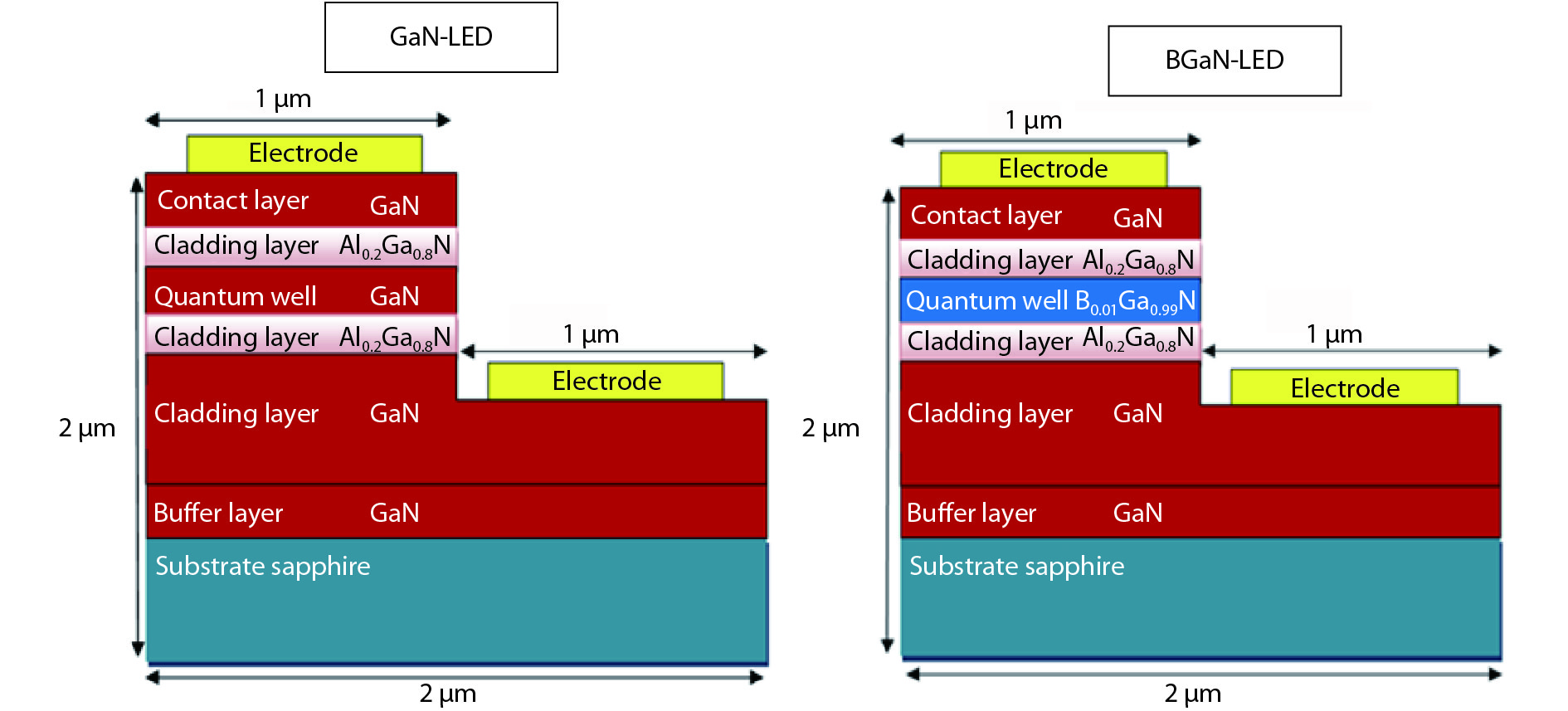
Fig. 1.
(Color online) Schematic structure of UV LEDs with GaN and BGaN single quantum well.
ARTICLES
Asma Belaid and Abdelkader Hamdoune
Corresponding author: Asma Belaid, Email: belaidaasma@gmail.com
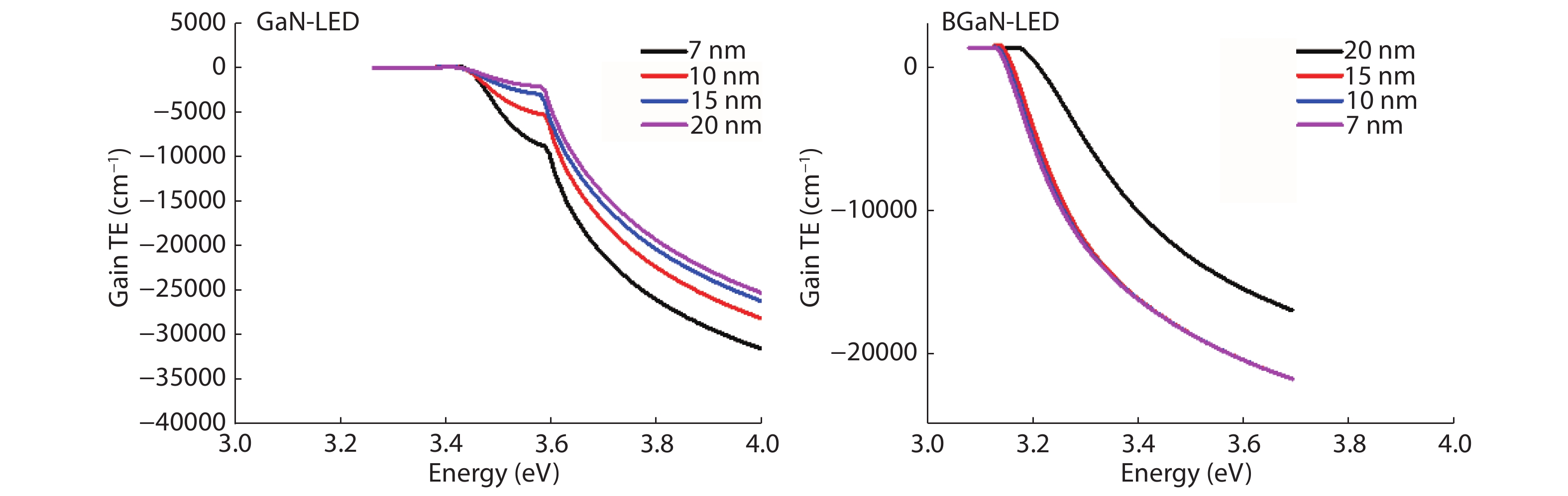
Abstract: The objective of this work is to simulate a single quantum well ultraviolet light emitting diode (LED) based on AlGaN/GaN/AlGaN and AlGaN/BGaN/AlGaN, by using TCAD Silvaco simulator. The first structure has a GaN quantum well taken between two layers, of n-AlGaN and p-AlGaN. The second one has a BGaN quantum well instead of GaN. We fix the concentration of the boron in BGaN to only 1% and we vary the thickness of GaN and BGaN quantum well layer from 7 to 20 nm, for the two structures. As results, we obtain respectively for GaN-LED and BGaN-LED, a maximum current of 0.52 and 0.27 mA, a maximum power spectral density of 1.935 and 6.7 W cm?1 eV?1, a maximum spontaneous emission of 3.34 × 1028 and 3.43 × 1028 s?1 cm?3 eV?1, and a maximum Light output power of 0.56 and 0.89 mW.
Key words: gallium nitride (GaN), aluminum gallium nitride (AlGaN), boron gallium nitride (BGaN), UV light emitting diode (LED)
| [1] |
Hamdoune A. Elaboration du nitrure de gallium, étude de ses propriétés et applications. Thesis of Doctorate, University of Abou-Bakr Belkaid, Tlemcen, Algeria, 2006
|
| [2] |
Nakamura S. III-V nitride based light-emitting devices. Solid State Communications, 1997. 102: 237 doi: 10.1016/S0038-1098(96)00722-3
|
| [3] |
Masui H, Nakamura S, DenBaars S P, et al. Nonpolar and semipolar III-nitride light-emitting diodes: achievements and challenges. IEEE Trans Electron Devices, 2010, 57: 88 doi: 10.1109/TED.2009.2033773
|
| [4] |
Hu H P, Zhou S J, Liu X T, et al. Effects of GaN/AlGaN/sputtered AlN nucleation layers on performance of GaN-based ultraviolet light-emitting diodes. J Scientific Reports, 2017, 7, 44627 doi: 10.1038/srep44627
|
| [5] |
Kneissl M, Kolbe T, Chua C, et al. Advances in group III-nitride-based deep UV light-emitting diode technology. J Semicond Sci Technol 2011, 26 , 014036 doi: 10.1088/0268-1242/26/1/014036
|
| [6] |
Kneissl M, Rass J. III nitride ultraviolet emitters. Springer Series in Materials Science 2016, 227, 1
|
| [7] |
Khan A, Balakrishnan K, Katona T. Ultraviolet light-emitting diodes based on group three nitrides. J Nat Photonics 2008, 2, 77 doi: 10.1038/nphoton.2007.293
|
| [8] |
Nakamura S, Krames M R. History of gallium-nitride-based light-emitting diodes for illumination. Proc IEEE, 2013, 101(10), 2211 doi: 10.1109/JPROC.2013.2274929
|
| [9] |
Verzellesi G , Saguatti D, Meneghini M, et al. Efficiency droop in InGaN/GaN blue light-emitting diodes: physic mechanisms remedies. J Appl Phys 2013, 114(7), 071101. doi: 10.1063/1.4816434
|
| [10] |
Yang W, Wang W, Lin Y, et al. Deposition of nonpolar mplane InGaN/GaN multiple quantum wells on LiGaO+(100) substrates. J Mater Chem C 2014, 2(5), 801 doi: 10.1039/C3TC31935K
|
| [11] |
Schubert M F, Xu J, Kim J K, et al. Polarization-matched GaInN/AlGaInN multi-quantum-well light-emitting diodes with reduced efficiency droop. Appl Phys Lett. 2008, 93(4), 041102. doi: 10.1063/1.2963029
|
| [12] |
Lin Z T, Wang H Y, Wang W L, et al. Employing low-temperature barriers to achieve strain-relaxed and high-performance GaN-based LEDs. J Opt Express, 2016, 24, 11886. doi: 10.1364/OE.24.011885
|
| [13] |
Hirayama H, Fujikawa S, Noguchi N, et al. 222–282 nm AlGaN and InAlGaN-based deep-UV LEDs fabricated on high-quality AlN on sapphire. J Phys Status Solidi A, 2009, 206, 1176 doi: 10.1002/pssa.v206:6
|
| [14] |
Takano T, Fujikawa S, Kondo Y, et al. Remarkable improvement in output power for an InAlGaN based ultraviolet LED by improving the crystalline quality of AlN/AlGaN templates. J Phys Status Solidi C, 2008, 5, 2102 doi: 10.1002/(ISSN)1610-1642
|
| [15] |
Lin Z T, Wang H T, Lin Y H, et al. Stress management on underlying GaN-based epitaxial films: A new vision for achieving high-performance LEDs on Si substrates. J Appl Phys, 2017, 122, 204503. doi: 10.1063/1.4993985
|
| [16] |
Meel K, Mahala P, Singh S. Design and fabrication of multi quantum well based GaN/InGaN blue LED. IOP Conf Ser: Mater Sci Eng, 2018, 331, 012008 doi: 10.1088/1757-899X/331/1/012008
|
| [17] |
Gautier S, Patriarche G, Moudakir T. Deep structural analysis of novel BGaN material layers grown by MOVPE. J Cryst Growth 2011, 315, 288 doi: 10.1016/j.jcrysgro.2010.08.042
|
| [18] |
Pease R S. An X-ray study of boron nitride. Acta Crystallogr. 1952, 5, 356. doi: 10.1107/S0365110X52001064
|
| [19] |
Herold A, Marzluf B, Perio P, et al. Inorganic reactions and methods. Formation of Ceramics Seances Acad Sci 1958, 246, 1866
|
| [20] |
Thomas J, Weston N E, O’connor T, et al. Boron nitride, thermal transformation to ordered-layer-lattice boron nitride. J Am Chem Soc 1962, 84, 4619. doi: 10.1021/ja00883a001
|
| [21] |
Wentorf R Jr. Cubic form of boron nitride. J Chem Phys, 1957, 26, 956. doi: 10.1063/1.1745964
|
| [22] |
Wentorf R Jr. Synthesis of the cubic form of boron nitride. J Chem Phys. 1961, 34, 809. doi: 10.1063/1.1731679
|
| [23] |
Tsao J Y, Chowdhury S, Hollis M A, et al. Ultrawide-bandgap semiconductors: research opportunities and challenges. J Adv Electron Mater. 2018, 4, 1600501 doi: 10.1002/aelm.201600501
|
| [24] |
Zhang X. Thin solid films electronic and photonic applications, 2013, 544, 2. doi: 10.1016/j.tsf.2013.07.001
|
| [25] |
Dreyer C E, Lyons J L, Janotti A, et al. Band alignments and polarization properties of BN polymorphs. Appl Phys Express, 2014, 7, 031001. doi: 10.7567/APEX.7.031001
|
| [26] |
Gunning B P, Moseley M W, Koleske D D, et al. Phase degradation in BxGa1-xN films grown at low temperature by metalorganic vapor phase epitaxy. J Cryst Growth, 2017, 464, 190. doi: 10.1016/j.jcrysgro.2016.10.054
|
| [27] |
Ougazzaden A, Gautier S, Moudakir T. Band gap bowing in BGaN thin films. Appl Phys Lett, 2008, 93, 083118 doi: 10.1063/1.2977588
|
| [28] |
Atlas User’s Manual; Silvaco International Inc. Santa Clara, CA, USA. Version: 2012
|
| [29] |
Lachebi A, Abid H, DrizMand Al-Douri Y. First-principles study of cubic BxGa1–xN alloys. Int J Nanoelectron, 2008, 1, 81 doi: 10.3906/.z-0902-3
|
| [30] |
Schubert E F. Light-emitting diodes. 2nd ed. Cambridge University Press, 2006, 432
|
| [31] |
Ambacher O, Dimitrov R, Stutzmann M, et al. Role of spontaneous and piezoelectric polarization induced effects in group-III nitride based heterostructures and devices. J Phys Stat Sol, 1999, 216, 381 doi: 10.1002/(ISSN)1521-3951
|
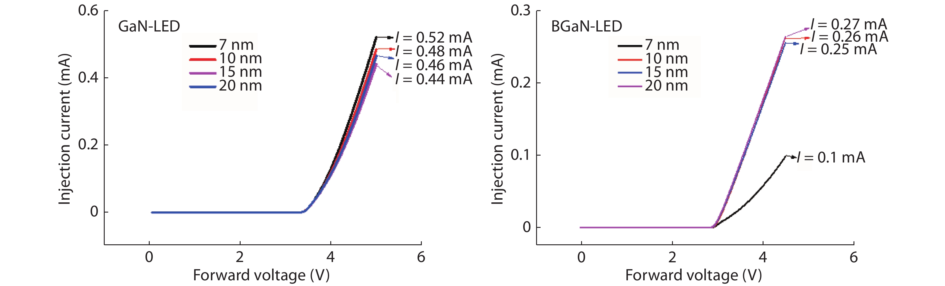
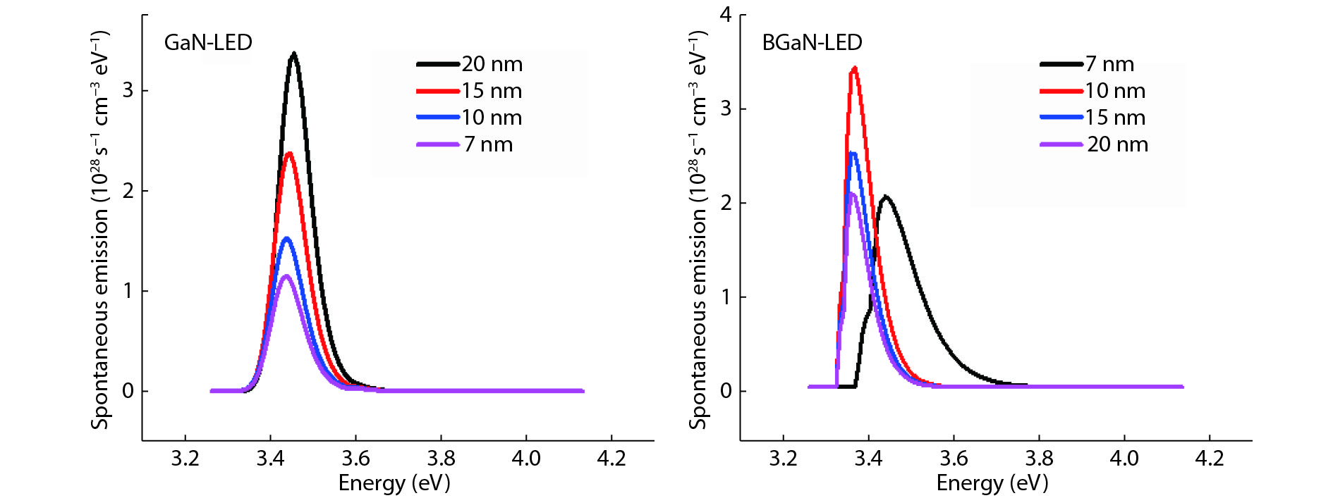
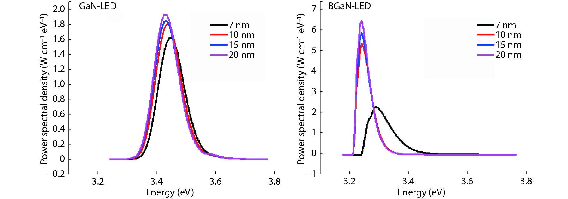
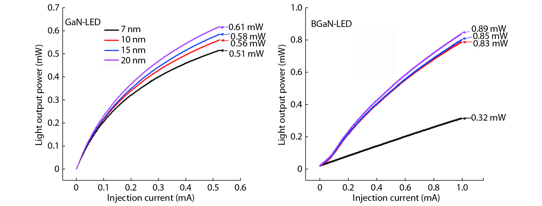
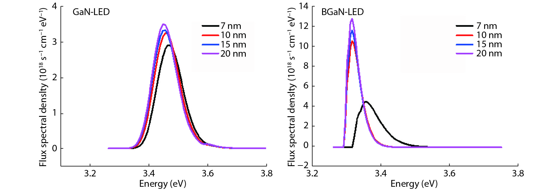
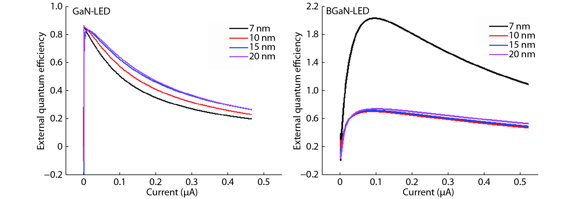
Table 1. Summarized values of spontaneous emission for GaN-LED and BGaN-LED.
| QW thickness (nm) | 7 | 10 | 15 | 20 | |
| GaN-LED | Peak energy (eV) | 3.43 | 3.43 | 3.44 | 3.45 |
| λ (nm) | 361.5 | 361.5 | 360.5 | 359.4 | |
| Spontaneous emission (1028 s?1 cm?3 eV?1) | 1.15 | 1.53 | 2.36 | 3.34 | |
| BGaN-LED | Peak energy (eV) | 3.43 | 3.36 | 3.36 | 3.36 |
| λ (nm) | 361.5 | 369 | 369 | 369 | |
| Spontaneous emission (1028 s?1 cm?3 eV?1) | 2.04 | 3.43 | 2.53 | 2.08 | |
| Ratio of spontaneous emissions | 1.77 | 2.24 | 1.07 | 0.62 | |
| Difference between spontaneous emissions (1028 s?1 cm?3 eV?1) | 0.89 | 1.9 | 0.17 | ?1.26 | |
 DownLoad: CSV
Table 2. Summarized values of power spectral density for GaN-LED and BGaN-LED.
| QW thickness (nm) | 7 | 10 | 15 | 20 | |
| GaN-LED | Peak energy (eV) | 3.46 | 3.45 | 3.45 | 3.45 |
| λ (nm) | 358.4 | 359.4 | 359.4 | 359.4 | |
| Power spectral density (W cm?1 eV?1) | 1.61 | 1.81 | 1.84 | 1.93 | |
| BGaN-LED | Peak energy (eV) | 3.35 | 3.31 | 3.31 | 3.31 |
| λ (nm) | 370.1 | 374.6 | 374.6 | 374.6 | |
| Power spectral density (W cm?1 eV?1) | 2.4 | 5.6 | 6.1 | 6.7 | |
| Ratio of power spectral densities | 1.49 | 3.09 | 3.31 | 3.47 | |
| Difference between power spectral densities (W cm?1 eV?1) | 0.79 | 3.79 | 4.26 | 4.77 | |
DownLoad: CSV
Table 3. Summarized values of flux spectral density for GaN-LED and BGaN-LED.
| QW thickness (nm) | 7 | 10 | 15 | 20 | |
| GaN-LED | Peak energy (eV) | 3.47 | 3.46 | 3.45 | 3.45 |
| λ (nm) | 357.3 | 358.4 | 359.4 | 359.4 | |
| Flux spectral density (1018 s?1 cm?1 eV?1) | 2.91 | 3.25 | 3.32 | 3.5 | |
| BGaN-LED | Peak energy (eV) | 3.35 | 3.31 | 3.31 | 3.31 |
| λ (nm) | 370.1 | 374.6 | 374.6 | 374.6 | |
| Flux spectral density (1018 s?1 cm?1 eV?1) | 4.48 | 10.3 | 11.3 | 12.5 | |
| Ratio of flux spectral densities (s?1 cm?1 eV?1) | 1.54 | 3.17 | 3.40 | 3.57 | |
| Difference between flux spectral densities (1018 s?1 cm?1 eV?1) | 1.57 | 7.05 | 7.98 | 9 | |
DownLoad: CSV
| [1] |
Hamdoune A. Elaboration du nitrure de gallium, étude de ses propriétés et applications. Thesis of Doctorate, University of Abou-Bakr Belkaid, Tlemcen, Algeria, 2006
|
| [2] |
Nakamura S. III-V nitride based light-emitting devices. Solid State Communications, 1997. 102: 237 doi: 10.1016/S0038-1098(96)00722-3
|
| [3] |
Masui H, Nakamura S, DenBaars S P, et al. Nonpolar and semipolar III-nitride light-emitting diodes: achievements and challenges. IEEE Trans Electron Devices, 2010, 57: 88 doi: 10.1109/TED.2009.2033773
|
| [4] |
Hu H P, Zhou S J, Liu X T, et al. Effects of GaN/AlGaN/sputtered AlN nucleation layers on performance of GaN-based ultraviolet light-emitting diodes. J Scientific Reports, 2017, 7, 44627 doi: 10.1038/srep44627
|
| [5] |
Kneissl M, Kolbe T, Chua C, et al. Advances in group III-nitride-based deep UV light-emitting diode technology. J Semicond Sci Technol 2011, 26 , 014036 doi: 10.1088/0268-1242/26/1/014036
|
| [6] |
Kneissl M, Rass J. III nitride ultraviolet emitters. Springer Series in Materials Science 2016, 227, 1
|
| [7] |
Khan A, Balakrishnan K, Katona T. Ultraviolet light-emitting diodes based on group three nitrides. J Nat Photonics 2008, 2, 77 doi: 10.1038/nphoton.2007.293
|
| [8] |
Nakamura S, Krames M R. History of gallium-nitride-based light-emitting diodes for illumination. Proc IEEE, 2013, 101(10), 2211 doi: 10.1109/JPROC.2013.2274929
|
| [9] |
Verzellesi G , Saguatti D, Meneghini M, et al. Efficiency droop in InGaN/GaN blue light-emitting diodes: physic mechanisms remedies. J Appl Phys 2013, 114(7), 071101. doi: 10.1063/1.4816434
|
| [10] |
Yang W, Wang W, Lin Y, et al. Deposition of nonpolar mplane InGaN/GaN multiple quantum wells on LiGaO+(100) substrates. J Mater Chem C 2014, 2(5), 801 doi: 10.1039/C3TC31935K
|
| [11] |
Schubert M F, Xu J, Kim J K, et al. Polarization-matched GaInN/AlGaInN multi-quantum-well light-emitting diodes with reduced efficiency droop. Appl Phys Lett. 2008, 93(4), 041102. doi: 10.1063/1.2963029
|
| [12] |
Lin Z T, Wang H Y, Wang W L, et al. Employing low-temperature barriers to achieve strain-relaxed and high-performance GaN-based LEDs. J Opt Express, 2016, 24, 11886. doi: 10.1364/OE.24.011885
|
| [13] |
Hirayama H, Fujikawa S, Noguchi N, et al. 222–282 nm AlGaN and InAlGaN-based deep-UV LEDs fabricated on high-quality AlN on sapphire. J Phys Status Solidi A, 2009, 206, 1176 doi: 10.1002/pssa.v206:6
|
| [14] |
Takano T, Fujikawa S, Kondo Y, et al. Remarkable improvement in output power for an InAlGaN based ultraviolet LED by improving the crystalline quality of AlN/AlGaN templates. J Phys Status Solidi C, 2008, 5, 2102 doi: 10.1002/(ISSN)1610-1642
|
| [15] |
Lin Z T, Wang H T, Lin Y H, et al. Stress management on underlying GaN-based epitaxial films: A new vision for achieving high-performance LEDs on Si substrates. J Appl Phys, 2017, 122, 204503. doi: 10.1063/1.4993985
|
| [16] |
Meel K, Mahala P, Singh S. Design and fabrication of multi quantum well based GaN/InGaN blue LED. IOP Conf Ser: Mater Sci Eng, 2018, 331, 012008 doi: 10.1088/1757-899X/331/1/012008
|
| [17] |
Gautier S, Patriarche G, Moudakir T. Deep structural analysis of novel BGaN material layers grown by MOVPE. J Cryst Growth 2011, 315, 288 doi: 10.1016/j.jcrysgro.2010.08.042
|
| [18] |
Pease R S. An X-ray study of boron nitride. Acta Crystallogr. 1952, 5, 356. doi: 10.1107/S0365110X52001064
|
| [19] |
Herold A, Marzluf B, Perio P, et al. Inorganic reactions and methods. Formation of Ceramics Seances Acad Sci 1958, 246, 1866
|
| [20] |
Thomas J, Weston N E, O’connor T, et al. Boron nitride, thermal transformation to ordered-layer-lattice boron nitride. J Am Chem Soc 1962, 84, 4619. doi: 10.1021/ja00883a001
|
| [21] |
Wentorf R Jr. Cubic form of boron nitride. J Chem Phys, 1957, 26, 956. doi: 10.1063/1.1745964
|
| [22] |
Wentorf R Jr. Synthesis of the cubic form of boron nitride. J Chem Phys. 1961, 34, 809. doi: 10.1063/1.1731679
|
| [23] |
Tsao J Y, Chowdhury S, Hollis M A, et al. Ultrawide-bandgap semiconductors: research opportunities and challenges. J Adv Electron Mater. 2018, 4, 1600501 doi: 10.1002/aelm.201600501
|
| [24] |
Zhang X. Thin solid films electronic and photonic applications, 2013, 544, 2. doi: 10.1016/j.tsf.2013.07.001
|
| [25] |
Dreyer C E, Lyons J L, Janotti A, et al. Band alignments and polarization properties of BN polymorphs. Appl Phys Express, 2014, 7, 031001. doi: 10.7567/APEX.7.031001
|
| [26] |
Gunning B P, Moseley M W, Koleske D D, et al. Phase degradation in BxGa1-xN films grown at low temperature by metalorganic vapor phase epitaxy. J Cryst Growth, 2017, 464, 190. doi: 10.1016/j.jcrysgro.2016.10.054
|
| [27] |
Ougazzaden A, Gautier S, Moudakir T. Band gap bowing in BGaN thin films. Appl Phys Lett, 2008, 93, 083118 doi: 10.1063/1.2977588
|
| [28] |
Atlas User’s Manual; Silvaco International Inc. Santa Clara, CA, USA. Version: 2012
|
| [29] |
Lachebi A, Abid H, DrizMand Al-Douri Y. First-principles study of cubic BxGa1–xN alloys. Int J Nanoelectron, 2008, 1, 81 doi: 10.3906/.z-0902-3
|
| [30] |
Schubert E F. Light-emitting diodes. 2nd ed. Cambridge University Press, 2006, 432
|
| [31] |
Ambacher O, Dimitrov R, Stutzmann M, et al. Role of spontaneous and piezoelectric polarization induced effects in group-III nitride based heterostructures and devices. J Phys Stat Sol, 1999, 216, 381 doi: 10.1002/(ISSN)1521-3951
|


Article views: 5002 Times PDF downloads: 205 Times Cited by: 0 Times
Received: 04 May 2018 Revised: 08 June 2018 Online: Accepted Manuscript: 11 January 2019Uncorrected proof: 11 January 2019Published: 01 March 2019
| Citation: |
Asma Belaid, Abdelkader Hamdoune. Numerical simulation of UV LEDs with GaN and BGaN single quantum well[J]. Journal of Semiconductors, 2019, 40(3): 032802. doi: 10.1088/1674-4926/40/3/032802
****
A Belaid, A Hamdoune, Numerical simulation of UV LEDs with GaN and BGaN single quantum well[J]. J. Semicond., 2019, 40(3): 032802. doi: 10.1088/1674-4926/40/3/032802.

|
| [1] |
Hamdoune A. Elaboration du nitrure de gallium, étude de ses propriétés et applications. Thesis of Doctorate, University of Abou-Bakr Belkaid, Tlemcen, Algeria, 2006
|
| [2] |
Nakamura S. III-V nitride based light-emitting devices. Solid State Communications, 1997. 102: 237 doi: 10.1016/S0038-1098(96)00722-3
|
| [3] |
Masui H, Nakamura S, DenBaars S P, et al. Nonpolar and semipolar III-nitride light-emitting diodes: achievements and challenges. IEEE Trans Electron Devices, 2010, 57: 88 doi: 10.1109/TED.2009.2033773
|
| [4] |
Hu H P, Zhou S J, Liu X T, et al. Effects of GaN/AlGaN/sputtered AlN nucleation layers on performance of GaN-based ultraviolet light-emitting diodes. J Scientific Reports, 2017, 7, 44627 doi: 10.1038/srep44627
|
| [5] |
Kneissl M, Kolbe T, Chua C, et al. Advances in group III-nitride-based deep UV light-emitting diode technology. J Semicond Sci Technol 2011, 26 , 014036 doi: 10.1088/0268-1242/26/1/014036
|
| [6] |
Kneissl M, Rass J. III nitride ultraviolet emitters. Springer Series in Materials Science 2016, 227, 1
|
| [7] |
Khan A, Balakrishnan K, Katona T. Ultraviolet light-emitting diodes based on group three nitrides. J Nat Photonics 2008, 2, 77 doi: 10.1038/nphoton.2007.293
|
| [8] |
Nakamura S, Krames M R. History of gallium-nitride-based light-emitting diodes for illumination. Proc IEEE, 2013, 101(10), 2211 doi: 10.1109/JPROC.2013.2274929
|
| [9] |
Verzellesi G , Saguatti D, Meneghini M, et al. Efficiency droop in InGaN/GaN blue light-emitting diodes: physic mechanisms remedies. J Appl Phys 2013, 114(7), 071101. doi: 10.1063/1.4816434
|
| [10] |
Yang W, Wang W, Lin Y, et al. Deposition of nonpolar mplane InGaN/GaN multiple quantum wells on LiGaO+(100) substrates. J Mater Chem C 2014, 2(5), 801 doi: 10.1039/C3TC31935K
|
| [11] |
Schubert M F, Xu J, Kim J K, et al. Polarization-matched GaInN/AlGaInN multi-quantum-well light-emitting diodes with reduced efficiency droop. Appl Phys Lett. 2008, 93(4), 041102. doi: 10.1063/1.2963029
|
| [12] |
Lin Z T, Wang H Y, Wang W L, et al. Employing low-temperature barriers to achieve strain-relaxed and high-performance GaN-based LEDs. J Opt Express, 2016, 24, 11886. doi: 10.1364/OE.24.011885
|
| [13] |
Hirayama H, Fujikawa S, Noguchi N, et al. 222–282 nm AlGaN and InAlGaN-based deep-UV LEDs fabricated on high-quality AlN on sapphire. J Phys Status Solidi A, 2009, 206, 1176 doi: 10.1002/pssa.v206:6
|
| [14] |
Takano T, Fujikawa S, Kondo Y, et al. Remarkable improvement in output power for an InAlGaN based ultraviolet LED by improving the crystalline quality of AlN/AlGaN templates. J Phys Status Solidi C, 2008, 5, 2102 doi: 10.1002/(ISSN)1610-1642
|
| [15] |
Lin Z T, Wang H T, Lin Y H, et al. Stress management on underlying GaN-based epitaxial films: A new vision for achieving high-performance LEDs on Si substrates. J Appl Phys, 2017, 122, 204503. doi: 10.1063/1.4993985
|
| [16] |
Meel K, Mahala P, Singh S. Design and fabrication of multi quantum well based GaN/InGaN blue LED. IOP Conf Ser: Mater Sci Eng, 2018, 331, 012008 doi: 10.1088/1757-899X/331/1/012008
|
| [17] |
Gautier S, Patriarche G, Moudakir T. Deep structural analysis of novel BGaN material layers grown by MOVPE. J Cryst Growth 2011, 315, 288 doi: 10.1016/j.jcrysgro.2010.08.042
|
| [18] |
Pease R S. An X-ray study of boron nitride. Acta Crystallogr. 1952, 5, 356. doi: 10.1107/S0365110X52001064
|
| [19] |
Herold A, Marzluf B, Perio P, et al. Inorganic reactions and methods. Formation of Ceramics Seances Acad Sci 1958, 246, 1866
|
| [20] |
Thomas J, Weston N E, O’connor T, et al. Boron nitride, thermal transformation to ordered-layer-lattice boron nitride. J Am Chem Soc 1962, 84, 4619. doi: 10.1021/ja00883a001
|
| [21] |
Wentorf R Jr. Cubic form of boron nitride. J Chem Phys, 1957, 26, 956. doi: 10.1063/1.1745964
|
| [22] |
Wentorf R Jr. Synthesis of the cubic form of boron nitride. J Chem Phys. 1961, 34, 809. doi: 10.1063/1.1731679
|
| [23] |
Tsao J Y, Chowdhury S, Hollis M A, et al. Ultrawide-bandgap semiconductors: research opportunities and challenges. J Adv Electron Mater. 2018, 4, 1600501 doi: 10.1002/aelm.201600501
|
| [24] |
Zhang X. Thin solid films electronic and photonic applications, 2013, 544, 2. doi: 10.1016/j.tsf.2013.07.001
|
| [25] |
Dreyer C E, Lyons J L, Janotti A, et al. Band alignments and polarization properties of BN polymorphs. Appl Phys Express, 2014, 7, 031001. doi: 10.7567/APEX.7.031001
|
| [26] |
Gunning B P, Moseley M W, Koleske D D, et al. Phase degradation in BxGa1-xN films grown at low temperature by metalorganic vapor phase epitaxy. J Cryst Growth, 2017, 464, 190. doi: 10.1016/j.jcrysgro.2016.10.054
|
| [27] |
Ougazzaden A, Gautier S, Moudakir T. Band gap bowing in BGaN thin films. Appl Phys Lett, 2008, 93, 083118 doi: 10.1063/1.2977588
|
| [28] |
Atlas User’s Manual; Silvaco International Inc. Santa Clara, CA, USA. Version: 2012
|
| [29] |
Lachebi A, Abid H, DrizMand Al-Douri Y. First-principles study of cubic BxGa1–xN alloys. Int J Nanoelectron, 2008, 1, 81 doi: 10.3906/.z-0902-3
|
| [30] |
Schubert E F. Light-emitting diodes. 2nd ed. Cambridge University Press, 2006, 432
|
| [31] |
Ambacher O, Dimitrov R, Stutzmann M, et al. Role of spontaneous and piezoelectric polarization induced effects in group-III nitride based heterostructures and devices. J Phys Stat Sol, 1999, 216, 381 doi: 10.1002/(ISSN)1521-3951
|

 WeChat ID
Journal of Semiconductors © 2017 All Rights Reserved 京ICP備05085259號-2