


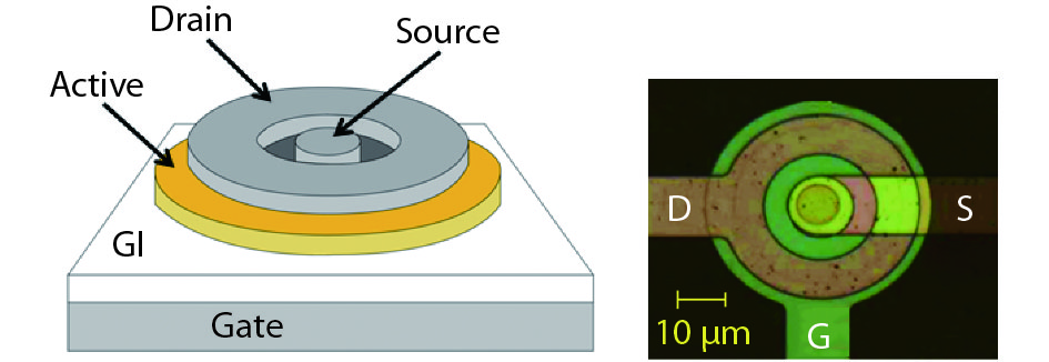
Fig. 1.
(Color online) (a) The schematic 3-D views and (b) optical image of the circular a-IGZO TFTs.
ARTICLES
Rui Geng1, and Yuxin Gong2
Corresponding author: Rui Geng, Email: gengrui@dlpu.edu.cn
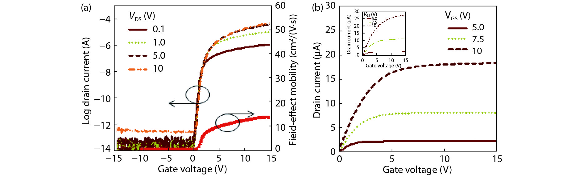
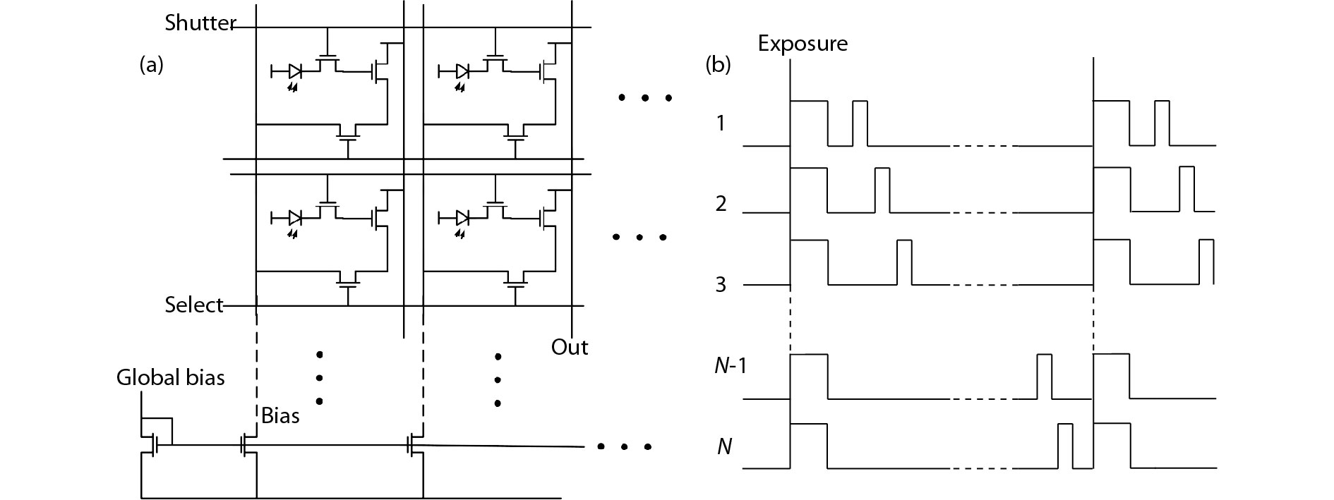
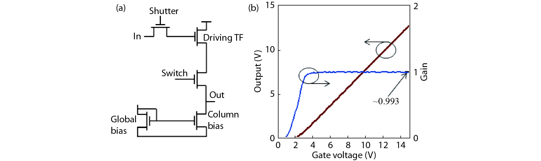
Abstract: We report a high-performance active image sensor pixel design by utilizing amorphous-indium-gallium-zinc-oxide (a-IGZO) thin-film transistors (TFTs) with a circular structure. The TFT, configured with the inner electrode as source and outer electrode as drain, typically exhibits good saturation electrical characteristics, where the device has a constant drive current despite variations in drain voltage. Due to the very high output resistance exhibited by this asymmetric TFT structure with a circular shape, the pixel circuit considered here in common-drain configuration provides a higher gain of operation than a pixel circuit implemented with rectangular a-IGZO TFTs. They can be used as driving TFTs in active image sensor circuits. They are, therefore, good candidates for digital X-ray detectors in applications such as medical diagnostic procedures.
Key words: a-IGZO TFT, active image sensor, circular structure, high gain
| [1] |
Kamiya T, Nomura K, Hosono H. Present status of amorphous IGZO thin-film transistors. Sci Technol Adv Mater, 2015, 11(4): 044305
|
| [2] |
Dayananda G K, Rai C S, Jayarama A, et al. Simulation model for electron irradiated IGZO thin film transistors. J Semicond, 2018, 39(2): 022002 doi: 10.1088/1674-4926/39/2/022002
|
| [3] |
Heo J S, Kim J H, Kim J K, et al. Photochemically activated flexible metal-oxide transistors and circuits using low impurity aqueous system. IEEE Electron Device Lett, 2015, 36(2): 162. doi: 10.1109/LED.2014.2382136
|
| [4] |
Petti L, Frutiger A, Münzenrieder N, et al. Flexible quasi-vertical In-Ga-Zn-O thin-film transistor with 300-nm channel length. IEEE Electron Device Lett, 2015, 36(5): 475. doi: 10.1109/LED.2015.2418295
|
| [5] |
Cantarella G, Münzenrieder N, Petti L, et al. Flexible In–Ga–Zn–O thin-film transistors on elastomeric substrate bent to 2.3% strain. IEEE Electron Device Lett, 2015, 36(8): 781. doi: 10.1109/LED.2015.2442271
|
| [6] |
Wang L T, Ou H, Chen J, et al. A numerical study of an amorphous silicon dual-gate photo thin-film transistor for low-dose X-ray imaging. J Display Technol, 2015, 11(8): 646. doi: 10.1109/JDT.2015.2403592
|
| [7] |
Gelinck G H, Kumar A, Moet D, et al. X-ray detector-on-plastic with high sensitivity using low cost, solution-processed organic photodiodes. IEEE Trans Electron Devices, 2016, 63(1): 197. doi: 10.1109/TED.2015.2432572
|
| [8] |
Ghittorelli M, Torricelli F, Kovács-Vajna Z M. Physical modeling of amorphous InGaZnO thin-film transistors: the role of degenerate conduction. IEEE Trans Electron Devices, 2016, 63(6): 2417. doi: 10.1109/TED.2016.2553963
|
| [9] |
Shao Y, Xiao X, He X, et al. Low-voltage a-InGaZnO thin-film transistors with anodized thin HfO2 gate dielectric. IEEE Electron Device Lett, 2015, 36(6): 573. doi: 10.1109/LED.2015.2422895
|
| [10] |
Kleinman D A, Schawlow A L. Corbino disk. J Appl Phys, 1960, 31(12): 2176. doi: 10.1063/1.1735520
|
| [11] |
Byun Y H, Boer W D, Yang M, et al. An amorphous silicon TFT with annular-shaped channel and reduced gate-source capacitance. IEEE Trans Electron Devices, 1996, 43(5): 839. doi: 10.1109/16.491263
|
| [12] |
Munteanu D, Cristoloveanu S, Hovel H. Circular pseudo-metal oxide semiconductor field effect transistor in silicon-on-insulator analytical model, simulation, and measurements. Electrochem Solid-State Lett, 1999, 2(5): 242. doi: 10.1149/1.1390798
|
| [13] |
Ker M D, Deng C K, Huang J L. On-panel output buffer with offset compensation technique for data driver in LTPS technology. J Display Technol, 2006, 2(2): 153. doi: 10.1109/JDT.2006.874510
|
| [14] |
Lin C L, Chen F H, Hung C C, et al. New a-IGZO pixel circuit composed of three transistors and one capacitor for use in high-speed-scan AMOLED displays. J Display Technol, 2015, 11(12): 1031. doi: 10.1109/JDT.2015.2494064
|
| [15] |
Cheng M H, Zhao C, Huang C L, et al. Amorphous InSnZnO thin-film transistor voltage-mode active pixel sensor circuits for indirect X-ray imagers. IEEE Trans Electron Devices, 2016, 63(12): 4802. doi: 10.1109/TED.2016.2615079
|


Article views: 4802 Times PDF downloads: 134 Times Cited by: 0 Times
Received: 16 July 2018 Revised: 14 September 2018 Online: Accepted Manuscript: 05 November 2018Uncorrected proof: 08 November 2018Published: 01 February 2019
| Citation: |
Rui Geng, Yuxin Gong. High performance active image sensor pixel design with circular structure oxide TFT[J]. Journal of Semiconductors, 2019, 40(2): 022402. doi: 10.1088/1674-4926/40/2/022402
****
R Geng, Y X Gong, High performance active image sensor pixel design with circular structure oxide TFT[J]. J. Semicond., 2019, 40(2): 022402. doi: 10.1088/1674-4926/40/2/022402.

|
| [1] |
Kamiya T, Nomura K, Hosono H. Present status of amorphous IGZO thin-film transistors. Sci Technol Adv Mater, 2015, 11(4): 044305
|
| [2] |
Dayananda G K, Rai C S, Jayarama A, et al. Simulation model for electron irradiated IGZO thin film transistors. J Semicond, 2018, 39(2): 022002 doi: 10.1088/1674-4926/39/2/022002
|
| [3] |
Heo J S, Kim J H, Kim J K, et al. Photochemically activated flexible metal-oxide transistors and circuits using low impurity aqueous system. IEEE Electron Device Lett, 2015, 36(2): 162. doi: 10.1109/LED.2014.2382136
|
| [4] |
Petti L, Frutiger A, Münzenrieder N, et al. Flexible quasi-vertical In-Ga-Zn-O thin-film transistor with 300-nm channel length. IEEE Electron Device Lett, 2015, 36(5): 475. doi: 10.1109/LED.2015.2418295
|
| [5] |
Cantarella G, Münzenrieder N, Petti L, et al. Flexible In–Ga–Zn–O thin-film transistors on elastomeric substrate bent to 2.3% strain. IEEE Electron Device Lett, 2015, 36(8): 781. doi: 10.1109/LED.2015.2442271
|
| [6] |
Wang L T, Ou H, Chen J, et al. A numerical study of an amorphous silicon dual-gate photo thin-film transistor for low-dose X-ray imaging. J Display Technol, 2015, 11(8): 646. doi: 10.1109/JDT.2015.2403592
|
| [7] |
Gelinck G H, Kumar A, Moet D, et al. X-ray detector-on-plastic with high sensitivity using low cost, solution-processed organic photodiodes. IEEE Trans Electron Devices, 2016, 63(1): 197. doi: 10.1109/TED.2015.2432572
|
| [8] |
Ghittorelli M, Torricelli F, Kovács-Vajna Z M. Physical modeling of amorphous InGaZnO thin-film transistors: the role of degenerate conduction. IEEE Trans Electron Devices, 2016, 63(6): 2417. doi: 10.1109/TED.2016.2553963
|
| [9] |
Shao Y, Xiao X, He X, et al. Low-voltage a-InGaZnO thin-film transistors with anodized thin HfO2 gate dielectric. IEEE Electron Device Lett, 2015, 36(6): 573. doi: 10.1109/LED.2015.2422895
|
| [10] |
Kleinman D A, Schawlow A L. Corbino disk. J Appl Phys, 1960, 31(12): 2176. doi: 10.1063/1.1735520
|
| [11] |
Byun Y H, Boer W D, Yang M, et al. An amorphous silicon TFT with annular-shaped channel and reduced gate-source capacitance. IEEE Trans Electron Devices, 1996, 43(5): 839. doi: 10.1109/16.491263
|
| [12] |
Munteanu D, Cristoloveanu S, Hovel H. Circular pseudo-metal oxide semiconductor field effect transistor in silicon-on-insulator analytical model, simulation, and measurements. Electrochem Solid-State Lett, 1999, 2(5): 242. doi: 10.1149/1.1390798
|
| [13] |
Ker M D, Deng C K, Huang J L. On-panel output buffer with offset compensation technique for data driver in LTPS technology. J Display Technol, 2006, 2(2): 153. doi: 10.1109/JDT.2006.874510
|
| [14] |
Lin C L, Chen F H, Hung C C, et al. New a-IGZO pixel circuit composed of three transistors and one capacitor for use in high-speed-scan AMOLED displays. J Display Technol, 2015, 11(12): 1031. doi: 10.1109/JDT.2015.2494064
|
| [15] |
Cheng M H, Zhao C, Huang C L, et al. Amorphous InSnZnO thin-film transistor voltage-mode active pixel sensor circuits for indirect X-ray imagers. IEEE Trans Electron Devices, 2016, 63(12): 4802. doi: 10.1109/TED.2016.2615079
|

 WeChat ID
Journal of Semiconductors © 2017 All Rights Reserved 京ICP備05085259號-2
 DownLoad:

