


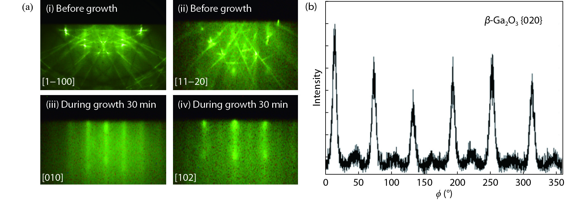
Fig. 1.
(Color online) (a) RHEED patterns before and after the deposition of β-Ga2O3 films. (b) XRD in-plane ? scan for the β-Ga2O3 film grown at substrate temperature of 630 °C.
ARTICLES
Jiaqi Wei, Kumsong Kim, Fang Liu, Ping Wang, Xiantong Zheng, Zhaoying Chen, Ding Wang, Ali Imran, Xin Rong, Xuelin Yang, Fujun Xu, Jing Yang, Bo Shen and Xinqiang Wang
Corresponding author: Xinqiang Wang, Email: wangshi@pku.edu.cn
Abstract: Monoclinic gallium oxide (Ga2O3) has been grown on (0001) sapphire (Al2O3) substrate by plasma-assisted molecular beam epitaxy (PA-MBE). The epitaxial relationship has been confirmed to be [010](
Key words: β-Ga2O3, sapphire substrate, PA-MBE, crystalline quality, CL measurement
| [1] |
Guo D, Wu Z, Li P, et al. Fabrication of β-Ga2O3 thin films and solar-blind photodetectors by laser MBE technology. Opt Mater Express, 2014, 4(5): 1067 doi: 10.1364/OME.4.001067
|
| [2] |
Mu W, Jia Z, Yin Y, et al. High quality crystal growth and anisotropic physical characterization of β-Ga2O3 single crystals grown by EFG method. J Alloys Compd, 2017, 714: 453 doi: 10.1016/j.jallcom.2017.04.185
|
| [3] |
Pearton S J, Yang J, Patrick C, et al. A review of Ga2O3 materials, processing, and devices. Appl Phys Rev, 2018, 5(1): 011301 doi: 10.1063/1.5006941
|
| [4] |
Xue H, He Q, Jian G, et al. An overview of the ultrawide bandgap Ga2O3 semiconductor-based schottky barrier diode for power electronics application. Nanoscale Res Lett, 2018 13: 290 doi: 10.1186/s11671-018-2712-1
|
| [5] |
Zhao X, Cui W, Wu Z, et al. Growth and characterization of Sn doped β-Ga2O3 thin films and enhanced performance in a solar-blind photodetector. J Electron Mater, 2017, 46(4): 2366 doi: 10.1007/s11664-017-5291-5
|
| [6] |
Kumar S S, Rubio E J, Noor-A-Alam M, et al. Structure, morphology, and optical properties of amorphous and nanocrystalline gallium oxide thin films. J Phys Chem C, 2013, 117(8): 4194 doi: 10.1021/jp311300e
|
| [7] |
Farzana E, Ahmadi E, Speck J S, et al. Deep level defects in Ge-doped (010) β-Ga2O3 layers grown by plasma-assisted molecular beam epitaxy. J Appl Phys, 2018, 123(16): 1
|
| [8] |
Hu Z, Zhou H, Feng Q, et al. Field-plated lateral β-Ga2O3 schottky barrier diode with high reverse blocking voltage of more than 3 kV and high DC power figure-of-merit of 500 MW/cm2. IEEE Electron Device Lett, 2018, 39(10): 1564
|
| [9] |
Higashiwaki M, Sasaki K, Kuramata A, et al. Development of gallium oxide power devices. Phys Status Solidi, 2014, 211(1): 21 doi: 10.1002/pssa.201330197
|
| [10] |
Galazka Z. β-Ga2O3 for wide-bandgap electronics and optoelectronics. Semicond Sci Technol, 2018, 33, 113001 doi: 10.1088/1361-6641/aadf78
|
| [11] |
Kumar S, Tessarek C, Christiansen S, et al. A comparative study of β-Ga2O3 nanowires grown on different substrates using CVD technique. J Alloys Compd, 2014, 587: 812 doi: 10.1016/j.jallcom.2013.10.165
|
| [12] |
Rafique S, Han L, Neal A T, et al. Towards high mobility heteroepitaxial β-Ga2O3 on sapphire-dependence on the substrate off-axis angle. Phys Status Solidi, 2018, 215(2): 1700467 doi: 10.1002/pssa.v215.2
|
| [13] |
E G Víllora, Shimamura K, Yoshikawa Y, et al. Large-size β-Ga2O3 single crystals and wafers. J Cryst Growth, 2004, 270(3/4): 420
|
| [14] |
Aida H, Nishiguchi K, Takeda H, et al. Growth of β-Ga2O3 single crystals by the edge-defined, film fed growth method. Jpn J Appl Phys, 2008, 47(11R): 8506
|
| [15] |
Higashiwaki M, Konishi K, Sasaki K, et al. Temperature-dependent capacitance-voltage and current-voltage characteristics of Pt/Ga2O3 (001) Schottky barrier diodes fabricated on n-Ga2O3 drift layers grown by halide vapor phase epitaxy. Appl Phys Lett, 2016, 108(13): 133503 doi: 10.1063/1.4945267
|
| [16] |
Sinha G, Adhikar K, Chaudhuri S, et al. Sol-gel derived phase pure α-Ga2O3 nanocrystalline thin film and its optical properties. J Cryst Growth, 2005, 276(1): 204
|
| [17] |
Kokubun Y, Miura K, Endo F, et al. Sol-gel prepared β-Ga2O3 thin films for ultraviolet photodetectors. Appl Phys Lett, 2007, 90(3): A316
|
| [18] |
Fleischer M, Hanrieder W, Meixner H. Stability of semiconducting gallium oxide thin films. Thin Solid Films, 1990, 190: 93 doi: 10.1016/0040-6090(90)90132-W
|
| [19] |
Liu J J, Yan J L, Shi L, et al. Electrical and optical properties of deep ultraviolet transparent conductive Ga2O3/ITO films by magnetron sputtering. J Semicond, 2010. 31: 103001. doi: 10.1088/1674-4926/31/10/103001
|
| [20] |
Ji Z, Du J, Fan J, et al. Gallium oxide films for filter and solar-blind UV detector. Opt Mater, 2006, 28(4): 415 doi: 10.1016/j.optmat.2005.03.006
|
| [21] |
Fleischer M, Hanrieder W, Meixner H. Stability of semiconducting gallium oxide thin films. Thin Solid Films, 2015, 190(1): 93
|
| [22] |
Lv Y, Ma J, Mi W, et al. Characterization of β-Ga2O3 thin films on sapphire (0001) using metal-organic chemical vapor deposition technique. Vacuum, 2012, 86(12): 1850 doi: 10.1016/j.vacuum.2012.04.019
|
| [23] |
Hayashi H, Huang R, Oba F, et al. Epitaxial growth of Mn-doped γ-Ga2O3 on spinel substrate. J Mater Res, 2011, 26(4): 578 doi: 10.1557/jmr.2010.32
|
| [24] |
Matsuzaki K, Hiramatsu H, Nomura K, et al. Growth, structure and carrier transport properties of Ga2O3 epitaxial film examined for transparent field-effect transistor. Thin Solid Films, 2006, 496(1): 37 doi: 10.1016/j.tsf.2005.08.187
|
| [25] |
Zhang F, Saito K, Tanaka T, et al. Electrical properties of Si doped Ga2O3 films grown by pulsed laser deposition. J Mater Sci: Mater Electron, 2015, 26(12): 9624 doi: 10.1007/s10854-015-3627-6
|
| [26] |
Oshima T, Okuno T, Fujita S. Ga2O3 thin film growth on c-plane sapphire substrates by molecular beam epitaxy for deep-ultraviolet photodetectors. Jpn J Appl Phys, 2007, 46(11): 7217 doi: 10.1143/JJAP.46.7217
|
| [27] |
Nakagomi S, Kokubun Y. Crystal orientation of β-Ga2O3 thin films formed on c-plane and a-plane sapphire substrate. J Cryst Growth, 2012, 349(1): 12 doi: 10.1016/j.jcrysgro.2012.04.006
|
| [28] |
Zhang Y, Joishi C, Xia Z, et al. Demonstration of β-(AlxGa1?x)2O3/Ga2O3 double heterostructure field effect transistors. Appl Phys Lett, 2018, 112(23): 233503 doi: 10.1063/1.5037095
|
| [29] |
Zhang F B, Saito K, Tanaka T, et al. Structural and optical properties of Ga2O3, films on sapphire substrates by pulsed laser deposition. J Cryst Growth, 2014, 387(2): 96
|
| [30] |
Huang L, Feng Q, Han G, et al. Comparison study of β-Ga2O3 photodetectors grown on sapphire at different oxygen pressures. IEEE Photonics J, 2017, 9(4): 1
|
| [31] |
Cheng Z, Hanke M, Vogt P, et al. Phase formation and strain relaxation of Ga2O3 on c-plane and a-plane sapphire substrates as studied by synchrotron-based x-ray diffraction. Appl Phys Lett, 2017, 111(16): 162104 doi: 10.1063/1.4998804
|
| [32] |
Villora E G, Shimamura K, Kitamura K, et al. Rf-plasma-assisted molecular-beam epitaxy of β-Ga2O3. Appl Phys Lett, 2006, 88(3): 841
|
| [33] |
Vogt P, Bierwagen O. Reaction kinetics and growth window for plasma-assisted molecular beam epitaxy of Ga2O3: Incorporation of Ga vs. Ga2O desorption. Appl Phys Lett, 2016, 108(7): 024001
|
| [34] |
Ravadgar P, Horng R H, Yao S D, et al. Effects of crystallinity and point defects on optoelectronic applications of β-Ga2O3 epilayers. Opt Express, 2013, 21(21): 24599 doi: 10.1364/OE.21.024599
|
| [35] |
Guzmán-Navarro G, Herrera-Zaldívar M, Valenzuela-Benavides J, et al. CL study of blue and UV emissions in β-Ga2O3 nanowires grown by thermal evaporation of GaN. J Appl Phys, 2011, 110(3): 033517 doi: 10.1063/1.3610386
|
| [36] |
Yu D P, Bubendorff J L, Zhou J F, et al. Localized cathodoluminescence investigation on single Ga2O3 nanoribbon/nanowire. Solid State Commun, 2002, 124(10/11): 417
|
| [37] |
Hao J, Cocivera M. Optical and luminescent properties of undoped and rare-earth-doped Ga2O3 thin films deposited by spray pyrolysis. J Phys D Appl Phys, 2002, 35(5): 433 doi: 10.1088/0022-3727/35/5/304
|


Article views: 6811 Times PDF downloads: 339 Times Cited by: 0 Times
Received: 02 September 2018 Revised: 10 November 2018 Online: Accepted Manuscript: 10 December 2018Uncorrected proof: 10 December 2018Published: 07 January 2019
| Citation: |
Jiaqi Wei, Kumsong Kim, Fang Liu, Ping Wang, Xiantong Zheng, Zhaoying Chen, Ding Wang, Ali Imran, Xin Rong, Xuelin Yang, Fujun Xu, Jing Yang, Bo Shen, Xinqiang Wang. β-Ga2O3 thin film grown on sapphire substrate by plasma-assisted molecular beam epitaxy[J]. Journal of Semiconductors, 2019, 40(1): 012802. doi: 10.1088/1674-4926/40/1/012802
****
J Q Wei, K Kim, F Liu, P Wang, X T Zheng, Z Y Chen, D Wang, A Imran, X Rong, X L Yang, F J Xu, J Yang, B Shen, X Q Wang, β-Ga2O3 thin film grown on sapphire substrate by plasma-assisted molecular beam epitaxy[J]. J. Semicond., 2019, 40(1): 012802. doi: 10.1088/1674-4926/40/1/012802.

|
| [1] |
Guo D, Wu Z, Li P, et al. Fabrication of β-Ga2O3 thin films and solar-blind photodetectors by laser MBE technology. Opt Mater Express, 2014, 4(5): 1067 doi: 10.1364/OME.4.001067
|
| [2] |
Mu W, Jia Z, Yin Y, et al. High quality crystal growth and anisotropic physical characterization of β-Ga2O3 single crystals grown by EFG method. J Alloys Compd, 2017, 714: 453 doi: 10.1016/j.jallcom.2017.04.185
|
| [3] |
Pearton S J, Yang J, Patrick C, et al. A review of Ga2O3 materials, processing, and devices. Appl Phys Rev, 2018, 5(1): 011301 doi: 10.1063/1.5006941
|
| [4] |
Xue H, He Q, Jian G, et al. An overview of the ultrawide bandgap Ga2O3 semiconductor-based schottky barrier diode for power electronics application. Nanoscale Res Lett, 2018 13: 290 doi: 10.1186/s11671-018-2712-1
|
| [5] |
Zhao X, Cui W, Wu Z, et al. Growth and characterization of Sn doped β-Ga2O3 thin films and enhanced performance in a solar-blind photodetector. J Electron Mater, 2017, 46(4): 2366 doi: 10.1007/s11664-017-5291-5
|
| [6] |
Kumar S S, Rubio E J, Noor-A-Alam M, et al. Structure, morphology, and optical properties of amorphous and nanocrystalline gallium oxide thin films. J Phys Chem C, 2013, 117(8): 4194 doi: 10.1021/jp311300e
|
| [7] |
Farzana E, Ahmadi E, Speck J S, et al. Deep level defects in Ge-doped (010) β-Ga2O3 layers grown by plasma-assisted molecular beam epitaxy. J Appl Phys, 2018, 123(16): 1
|
| [8] |
Hu Z, Zhou H, Feng Q, et al. Field-plated lateral β-Ga2O3 schottky barrier diode with high reverse blocking voltage of more than 3 kV and high DC power figure-of-merit of 500 MW/cm2. IEEE Electron Device Lett, 2018, 39(10): 1564
|
| [9] |
Higashiwaki M, Sasaki K, Kuramata A, et al. Development of gallium oxide power devices. Phys Status Solidi, 2014, 211(1): 21 doi: 10.1002/pssa.201330197
|
| [10] |
Galazka Z. β-Ga2O3 for wide-bandgap electronics and optoelectronics. Semicond Sci Technol, 2018, 33, 113001 doi: 10.1088/1361-6641/aadf78
|
| [11] |
Kumar S, Tessarek C, Christiansen S, et al. A comparative study of β-Ga2O3 nanowires grown on different substrates using CVD technique. J Alloys Compd, 2014, 587: 812 doi: 10.1016/j.jallcom.2013.10.165
|
| [12] |
Rafique S, Han L, Neal A T, et al. Towards high mobility heteroepitaxial β-Ga2O3 on sapphire-dependence on the substrate off-axis angle. Phys Status Solidi, 2018, 215(2): 1700467 doi: 10.1002/pssa.v215.2
|
| [13] |
E G Víllora, Shimamura K, Yoshikawa Y, et al. Large-size β-Ga2O3 single crystals and wafers. J Cryst Growth, 2004, 270(3/4): 420
|
| [14] |
Aida H, Nishiguchi K, Takeda H, et al. Growth of β-Ga2O3 single crystals by the edge-defined, film fed growth method. Jpn J Appl Phys, 2008, 47(11R): 8506
|
| [15] |
Higashiwaki M, Konishi K, Sasaki K, et al. Temperature-dependent capacitance-voltage and current-voltage characteristics of Pt/Ga2O3 (001) Schottky barrier diodes fabricated on n-Ga2O3 drift layers grown by halide vapor phase epitaxy. Appl Phys Lett, 2016, 108(13): 133503 doi: 10.1063/1.4945267
|
| [16] |
Sinha G, Adhikar K, Chaudhuri S, et al. Sol-gel derived phase pure α-Ga2O3 nanocrystalline thin film and its optical properties. J Cryst Growth, 2005, 276(1): 204
|
| [17] |
Kokubun Y, Miura K, Endo F, et al. Sol-gel prepared β-Ga2O3 thin films for ultraviolet photodetectors. Appl Phys Lett, 2007, 90(3): A316
|
| [18] |
Fleischer M, Hanrieder W, Meixner H. Stability of semiconducting gallium oxide thin films. Thin Solid Films, 1990, 190: 93 doi: 10.1016/0040-6090(90)90132-W
|
| [19] |
Liu J J, Yan J L, Shi L, et al. Electrical and optical properties of deep ultraviolet transparent conductive Ga2O3/ITO films by magnetron sputtering. J Semicond, 2010. 31: 103001. doi: 10.1088/1674-4926/31/10/103001
|
| [20] |
Ji Z, Du J, Fan J, et al. Gallium oxide films for filter and solar-blind UV detector. Opt Mater, 2006, 28(4): 415 doi: 10.1016/j.optmat.2005.03.006
|
| [21] |
Fleischer M, Hanrieder W, Meixner H. Stability of semiconducting gallium oxide thin films. Thin Solid Films, 2015, 190(1): 93
|
| [22] |
Lv Y, Ma J, Mi W, et al. Characterization of β-Ga2O3 thin films on sapphire (0001) using metal-organic chemical vapor deposition technique. Vacuum, 2012, 86(12): 1850 doi: 10.1016/j.vacuum.2012.04.019
|
| [23] |
Hayashi H, Huang R, Oba F, et al. Epitaxial growth of Mn-doped γ-Ga2O3 on spinel substrate. J Mater Res, 2011, 26(4): 578 doi: 10.1557/jmr.2010.32
|
| [24] |
Matsuzaki K, Hiramatsu H, Nomura K, et al. Growth, structure and carrier transport properties of Ga2O3 epitaxial film examined for transparent field-effect transistor. Thin Solid Films, 2006, 496(1): 37 doi: 10.1016/j.tsf.2005.08.187
|
| [25] |
Zhang F, Saito K, Tanaka T, et al. Electrical properties of Si doped Ga2O3 films grown by pulsed laser deposition. J Mater Sci: Mater Electron, 2015, 26(12): 9624 doi: 10.1007/s10854-015-3627-6
|
| [26] |
Oshima T, Okuno T, Fujita S. Ga2O3 thin film growth on c-plane sapphire substrates by molecular beam epitaxy for deep-ultraviolet photodetectors. Jpn J Appl Phys, 2007, 46(11): 7217 doi: 10.1143/JJAP.46.7217
|
| [27] |
Nakagomi S, Kokubun Y. Crystal orientation of β-Ga2O3 thin films formed on c-plane and a-plane sapphire substrate. J Cryst Growth, 2012, 349(1): 12 doi: 10.1016/j.jcrysgro.2012.04.006
|
| [28] |
Zhang Y, Joishi C, Xia Z, et al. Demonstration of β-(AlxGa1?x)2O3/Ga2O3 double heterostructure field effect transistors. Appl Phys Lett, 2018, 112(23): 233503 doi: 10.1063/1.5037095
|
| [29] |
Zhang F B, Saito K, Tanaka T, et al. Structural and optical properties of Ga2O3, films on sapphire substrates by pulsed laser deposition. J Cryst Growth, 2014, 387(2): 96
|
| [30] |
Huang L, Feng Q, Han G, et al. Comparison study of β-Ga2O3 photodetectors grown on sapphire at different oxygen pressures. IEEE Photonics J, 2017, 9(4): 1
|
| [31] |
Cheng Z, Hanke M, Vogt P, et al. Phase formation and strain relaxation of Ga2O3 on c-plane and a-plane sapphire substrates as studied by synchrotron-based x-ray diffraction. Appl Phys Lett, 2017, 111(16): 162104 doi: 10.1063/1.4998804
|
| [32] |
Villora E G, Shimamura K, Kitamura K, et al. Rf-plasma-assisted molecular-beam epitaxy of β-Ga2O3. Appl Phys Lett, 2006, 88(3): 841
|
| [33] |
Vogt P, Bierwagen O. Reaction kinetics and growth window for plasma-assisted molecular beam epitaxy of Ga2O3: Incorporation of Ga vs. Ga2O desorption. Appl Phys Lett, 2016, 108(7): 024001
|
| [34] |
Ravadgar P, Horng R H, Yao S D, et al. Effects of crystallinity and point defects on optoelectronic applications of β-Ga2O3 epilayers. Opt Express, 2013, 21(21): 24599 doi: 10.1364/OE.21.024599
|
| [35] |
Guzmán-Navarro G, Herrera-Zaldívar M, Valenzuela-Benavides J, et al. CL study of blue and UV emissions in β-Ga2O3 nanowires grown by thermal evaporation of GaN. J Appl Phys, 2011, 110(3): 033517 doi: 10.1063/1.3610386
|
| [36] |
Yu D P, Bubendorff J L, Zhou J F, et al. Localized cathodoluminescence investigation on single Ga2O3 nanoribbon/nanowire. Solid State Commun, 2002, 124(10/11): 417
|
| [37] |
Hao J, Cocivera M. Optical and luminescent properties of undoped and rare-earth-doped Ga2O3 thin films deposited by spray pyrolysis. J Phys D Appl Phys, 2002, 35(5): 433 doi: 10.1088/0022-3727/35/5/304
|

 WeChat ID
Journal of Semiconductors © 2017 All Rights Reserved 京ICP備05085259號-2
 DownLoad:

