


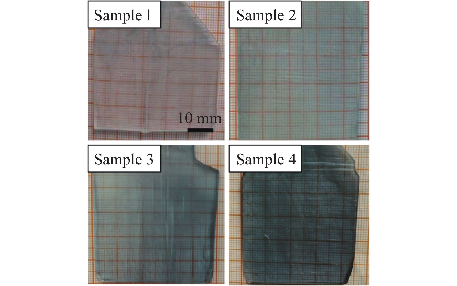
Fig. 1.
(Color online) The appearance of as-grown β-Ga2O3 single crystals. Sample 1 represents unintentionally doped β-Ga2O3 crystal and Sample 2 to Sample 4 represent Si-doped β-Ga2O3 single crystals with an increasing Si content.
SEMICONDUCTOR MATERIALS
Shengnan Zhang, Xiaozheng Lian, Yanchao Ma, Weidan Liu, Yingwu Zhang, Yongkuan Xu and Hongjuan Cheng
Corresponding author: Hongjuan Cheng, Email: xiemn08@126.com
Abstract: β-Ga2O3 is an ultra-wide band-gap semiconductor with promising applications in UV optical detectors, Schottky barrier diodes, field-effect transistors and substrates for light-emitting diodes. However, the preparation of large β-Ga2O3 crystals is undeveloped and many properties of this material have not been discovered yet. In this work, 2-inch β-Ga2O3 single crystals were grown by using an edge-defined film-fed growth method. The high quality of the crystal has been proved by high-resolution X-ray diffraction with 19.06 arcsec of the full width at half maximum. The electrical properties and optical properties of both the unintentionally doped and Si-doped β-Ga2O3 crystals were investigated systematically.
Key words: β-Ga2O3 single crystal, high quality, doping, electrical properties, optical properties
| [1] |
Kuramata A, Koshi K, Watanabe S, et al. High-quality β-Ga2O3 single crystals grown by edge-defined film-fed growth. Appl Phys Lett, 2016, 55(12): 1202A2
|
| [2] |
Onuma T, Fujioka S, Yamaguchi T, et al. Correlation between blue luminescence intensity and resistivity in β-Ga2O3 single crystals. Appl Phys Lett, 2013, 103(4): 3561
|
| [3] |
Galazka Z, Uecker R, Irmscher K, et al. Czochralski growth and characterization of β-Ga2O3 single crystals. Cryst Res Technol, 2010, 45(12): 1229 doi: 10.1002/crat.v45.12
|
| [4] |
Higashiwaki M, Murakami H, Kumagai Y, et al. Current status of Ga2O3 power devices. Jpn J Appl Phys, 2016, 55(12): 1202A1 doi: 10.7567/JJAP.55.1202A1
|
| [5] |
Suzuki R, Nakagomi S, Kokubun Y, et al. Enhancement of responsivity in solar-blind β-Ga2O3 photodiodes with a Au Schottky contact fabricated on single crystal substrates by annealing. Appl Phys Lett, 2009, 94(22): A316
|
| [6] |
Shimamura K, Villora E G, Domen K, et al. Epitaxial growth of GaN on (100) β-Ga2O3 substrates by metalorganic vapor phase epitaxy. Jpn J Appl Phys, 2005, 44: L7 doi: 10.1143/JJAP.44.L7
|
| [7] |
Higashiwaki M, Konishi K, Sasaki K, et al. Temperature-dependent capacitance-voltage and current-voltage characteristics of Pt/ Ga2O3 (001) Schottky barrier diodes fabricated on n-Ga2O3 drift layers grown by halide vapor phase epitaxy. Appl Phys Lett, 2016, 108(13): 1759
|
| [8] |
Wong M H, Sasaki K, Kuramata A, et al. Field-plated Ga2O3 MOSFETs with a breakdown voltage of over 750 V. IEEE Electron Device Lett, 2015, 37(2): 212
|
| [9] |
Galazka Z, Irmscher K, Uecker R, et al. On the bulk β-Ga2O3 single crystals grown by the Czochralski method. J Cryst Growth, 2014, 404(6): 184
|
| [10] |
Liu X, Qiu G, Zhao Y, et al. Gallium oxide nanorods by the conversion of gallium oxide hydroxide nanorods. J Alloys Compd, 2007, 439(1): 275
|
| [11] |
Filippo E, Tepore M, Baldassarre F, et al. Synthesis of β-Ga2O3 microstructures with efficient photocatalytic activity by annealing of GaSe single crystal. Appl Surf Sci, 2015, 338: 69 doi: 10.1016/j.apsusc.2015.02.105
|
| [12] |
Onuma T, Fujiok S. Polarized Raman spectra in β-Ga2O3 single crystals. J Cryst Growth, 2014, 401: 330 doi: 10.1016/j.jcrysgro.2013.12.061
|
| [13] |
Zhang Z, Farzana E, Arehart A, et al. Deep level defects throughout the bandgap of (010) β-Ga2O3 detected by optically and thermally stimulated defect spectroscopy. Appl Phys Lett, 2016, 108(7): 052105
|
| [14] |
Víllora E, Shimamura K, Yoshikawa Y, et al. Electrical conductivity and carrier concentration control in β-Ga2O3 by Si doping. Appl Phys Lett, 2008, 92(20): A316
|
| [15] |
Wang X, Zhang F, Saito K, et al. Electrical properties and emission mechanisms of Zn-doped β-Ga2O3 films. J Phys Chem Solids, 2014, 75(11): 1201 doi: 10.1016/j.jpcs.2014.06.005
|
| [16] |
Harwig T, Kellendonk F, and Slappendel S. The ultraviolet luminescence of β-galliumsesquioxide. J Phys Chem Solids, 1978, 39(6): 675 doi: 10.1016/0022-3697(78)90183-X
|
| [17] |
Takakura K, Koga D, Ohyama H, et al. Evaluation of the crystalline quality of β-Ga2O3, films by optical absorption measurements. Physica B, 2009, 404(23/24): 4854
|
| [18] |
Zhang Y J, Yan J L, Zhao G, et al. First principles calculation and experimental research of Si-doped β-Ga2O3. Acta Phys Sin, 2011, 60(3): 037103
|
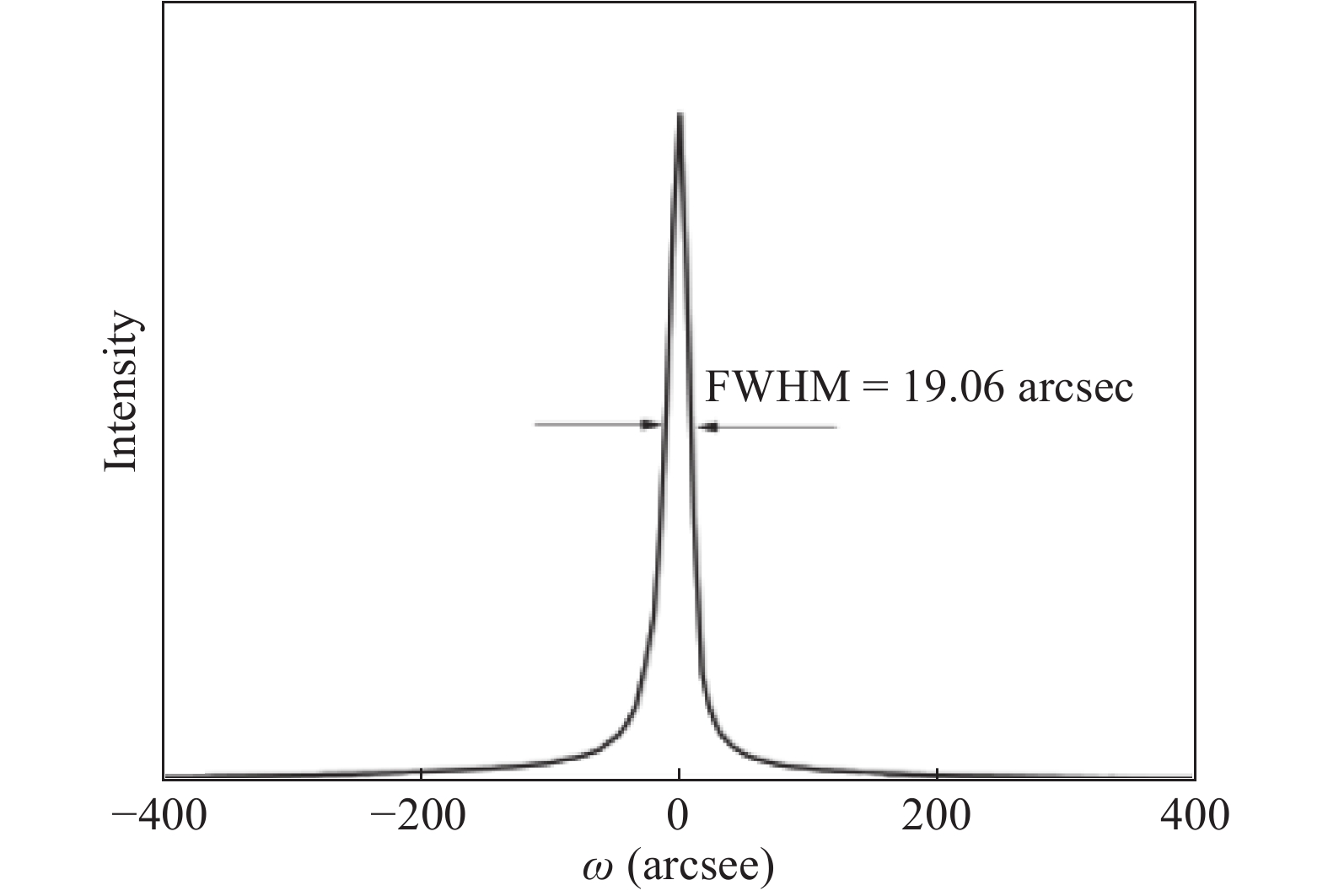
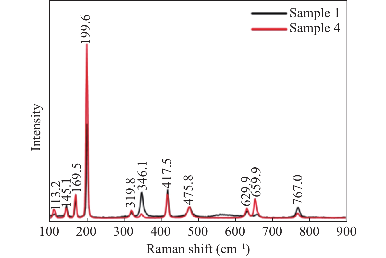
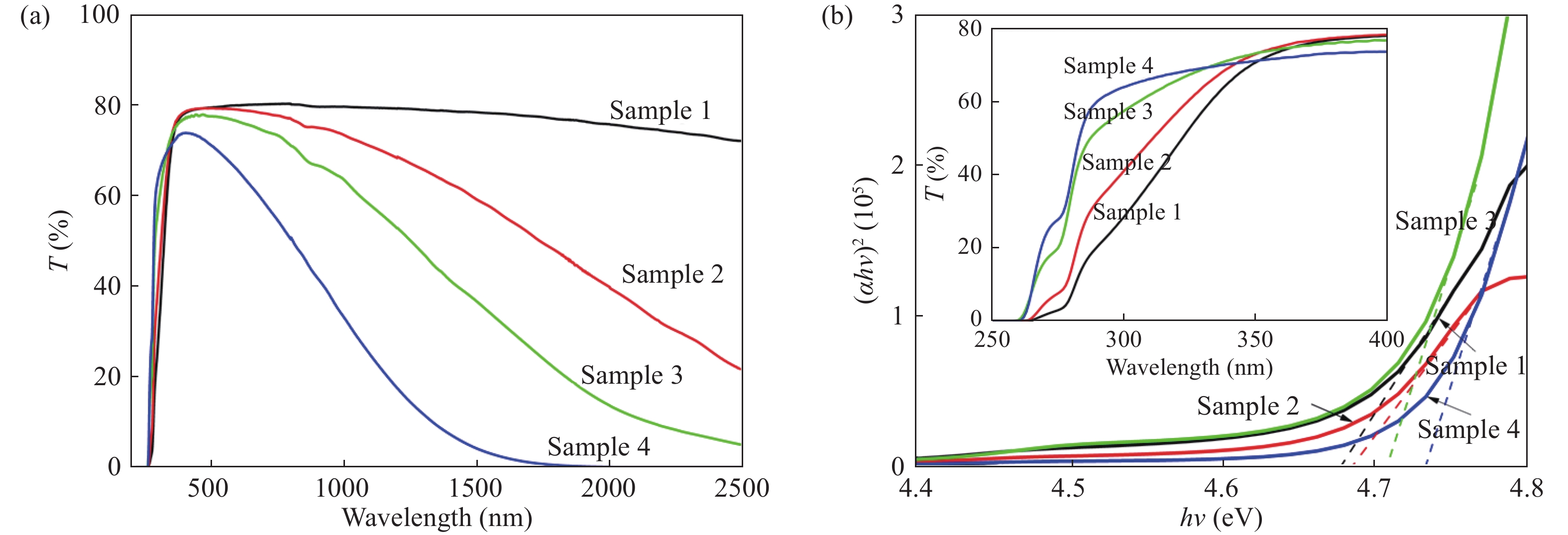
Table 1. The number of samples and the corresponding doping content of SiO2 power.
| Number of samples | Doping content of SiO2 power/100 g Ga2O3 power (mg) |
| Sample 1 | 0 |
| Sample 2 | 0.5 |
| Sample 3 | 4.0 |
| Sample 4 | 15.0 |
 DownLoad: CSV
Table 2. The Hall test results of EFG grown unintentionally doped and Si-doped β-Ga2O3 crystal.
| Sample | Resistivity (Ω·cm) | Mobility (cm2/(V·s)) | Carrier concentration (cm?3) | Conductive type |
| Sample 1 | 1.10 | 109 | 5.22 × 10¹⁶ | N |
| Sample 2 | 0.259 | 123 | 2.55 × 10¹⁷ | N |
| Sample 3 | 0.042 | 96 | 1.71 × 10¹⁸ | N |
| Sample 4 | 0.013 | 90 | 6.12 × 10¹⁸ | N |
DownLoad: CSV
| [1] |
Kuramata A, Koshi K, Watanabe S, et al. High-quality β-Ga2O3 single crystals grown by edge-defined film-fed growth. Appl Phys Lett, 2016, 55(12): 1202A2
|
| [2] |
Onuma T, Fujioka S, Yamaguchi T, et al. Correlation between blue luminescence intensity and resistivity in β-Ga2O3 single crystals. Appl Phys Lett, 2013, 103(4): 3561
|
| [3] |
Galazka Z, Uecker R, Irmscher K, et al. Czochralski growth and characterization of β-Ga2O3 single crystals. Cryst Res Technol, 2010, 45(12): 1229 doi: 10.1002/crat.v45.12
|
| [4] |
Higashiwaki M, Murakami H, Kumagai Y, et al. Current status of Ga2O3 power devices. Jpn J Appl Phys, 2016, 55(12): 1202A1 doi: 10.7567/JJAP.55.1202A1
|
| [5] |
Suzuki R, Nakagomi S, Kokubun Y, et al. Enhancement of responsivity in solar-blind β-Ga2O3 photodiodes with a Au Schottky contact fabricated on single crystal substrates by annealing. Appl Phys Lett, 2009, 94(22): A316
|
| [6] |
Shimamura K, Villora E G, Domen K, et al. Epitaxial growth of GaN on (100) β-Ga2O3 substrates by metalorganic vapor phase epitaxy. Jpn J Appl Phys, 2005, 44: L7 doi: 10.1143/JJAP.44.L7
|
| [7] |
Higashiwaki M, Konishi K, Sasaki K, et al. Temperature-dependent capacitance-voltage and current-voltage characteristics of Pt/ Ga2O3 (001) Schottky barrier diodes fabricated on n-Ga2O3 drift layers grown by halide vapor phase epitaxy. Appl Phys Lett, 2016, 108(13): 1759
|
| [8] |
Wong M H, Sasaki K, Kuramata A, et al. Field-plated Ga2O3 MOSFETs with a breakdown voltage of over 750 V. IEEE Electron Device Lett, 2015, 37(2): 212
|
| [9] |
Galazka Z, Irmscher K, Uecker R, et al. On the bulk β-Ga2O3 single crystals grown by the Czochralski method. J Cryst Growth, 2014, 404(6): 184
|
| [10] |
Liu X, Qiu G, Zhao Y, et al. Gallium oxide nanorods by the conversion of gallium oxide hydroxide nanorods. J Alloys Compd, 2007, 439(1): 275
|
| [11] |
Filippo E, Tepore M, Baldassarre F, et al. Synthesis of β-Ga2O3 microstructures with efficient photocatalytic activity by annealing of GaSe single crystal. Appl Surf Sci, 2015, 338: 69 doi: 10.1016/j.apsusc.2015.02.105
|
| [12] |
Onuma T, Fujiok S. Polarized Raman spectra in β-Ga2O3 single crystals. J Cryst Growth, 2014, 401: 330 doi: 10.1016/j.jcrysgro.2013.12.061
|
| [13] |
Zhang Z, Farzana E, Arehart A, et al. Deep level defects throughout the bandgap of (010) β-Ga2O3 detected by optically and thermally stimulated defect spectroscopy. Appl Phys Lett, 2016, 108(7): 052105
|
| [14] |
Víllora E, Shimamura K, Yoshikawa Y, et al. Electrical conductivity and carrier concentration control in β-Ga2O3 by Si doping. Appl Phys Lett, 2008, 92(20): A316
|
| [15] |
Wang X, Zhang F, Saito K, et al. Electrical properties and emission mechanisms of Zn-doped β-Ga2O3 films. J Phys Chem Solids, 2014, 75(11): 1201 doi: 10.1016/j.jpcs.2014.06.005
|
| [16] |
Harwig T, Kellendonk F, and Slappendel S. The ultraviolet luminescence of β-galliumsesquioxide. J Phys Chem Solids, 1978, 39(6): 675 doi: 10.1016/0022-3697(78)90183-X
|
| [17] |
Takakura K, Koga D, Ohyama H, et al. Evaluation of the crystalline quality of β-Ga2O3, films by optical absorption measurements. Physica B, 2009, 404(23/24): 4854
|
| [18] |
Zhang Y J, Yan J L, Zhao G, et al. First principles calculation and experimental research of Si-doped β-Ga2O3. Acta Phys Sin, 2011, 60(3): 037103
|


Article views: 6714 Times PDF downloads: 217 Times Cited by: 0 Times
Received: 01 December 2017 Revised: 28 February 2018 Online: Uncorrected proof: 20 April 2018Accepted Manuscript: 26 April 2018Published: 09 August 2018
| Citation: |
Shengnan Zhang, Xiaozheng Lian, Yanchao Ma, Weidan Liu, Yingwu Zhang, Yongkuan Xu, Hongjuan Cheng. Growth and characterization of 2-inch high quality β-Ga2O3 single crystals grown by EFG method[J]. Journal of Semiconductors, 2018, 39(8): 083003. doi: 10.1088/1674-4926/39/8/083003
****
S N Zhang, X Z Lian, Y C Ma, W D Liu, Y W Zhang, Y K Xu, H J Cheng, Growth and characterization of 2-inch high quality β-Ga2O3 single crystals grown by EFG method[J]. J. Semicond., 2018, 39(8): 083003. doi: 10.1088/1674-4926/39/8/083003.

|
| [1] |
Kuramata A, Koshi K, Watanabe S, et al. High-quality β-Ga2O3 single crystals grown by edge-defined film-fed growth. Appl Phys Lett, 2016, 55(12): 1202A2
|
| [2] |
Onuma T, Fujioka S, Yamaguchi T, et al. Correlation between blue luminescence intensity and resistivity in β-Ga2O3 single crystals. Appl Phys Lett, 2013, 103(4): 3561
|
| [3] |
Galazka Z, Uecker R, Irmscher K, et al. Czochralski growth and characterization of β-Ga2O3 single crystals. Cryst Res Technol, 2010, 45(12): 1229 doi: 10.1002/crat.v45.12
|
| [4] |
Higashiwaki M, Murakami H, Kumagai Y, et al. Current status of Ga2O3 power devices. Jpn J Appl Phys, 2016, 55(12): 1202A1 doi: 10.7567/JJAP.55.1202A1
|
| [5] |
Suzuki R, Nakagomi S, Kokubun Y, et al. Enhancement of responsivity in solar-blind β-Ga2O3 photodiodes with a Au Schottky contact fabricated on single crystal substrates by annealing. Appl Phys Lett, 2009, 94(22): A316
|
| [6] |
Shimamura K, Villora E G, Domen K, et al. Epitaxial growth of GaN on (100) β-Ga2O3 substrates by metalorganic vapor phase epitaxy. Jpn J Appl Phys, 2005, 44: L7 doi: 10.1143/JJAP.44.L7
|
| [7] |
Higashiwaki M, Konishi K, Sasaki K, et al. Temperature-dependent capacitance-voltage and current-voltage characteristics of Pt/ Ga2O3 (001) Schottky barrier diodes fabricated on n-Ga2O3 drift layers grown by halide vapor phase epitaxy. Appl Phys Lett, 2016, 108(13): 1759
|
| [8] |
Wong M H, Sasaki K, Kuramata A, et al. Field-plated Ga2O3 MOSFETs with a breakdown voltage of over 750 V. IEEE Electron Device Lett, 2015, 37(2): 212
|
| [9] |
Galazka Z, Irmscher K, Uecker R, et al. On the bulk β-Ga2O3 single crystals grown by the Czochralski method. J Cryst Growth, 2014, 404(6): 184
|
| [10] |
Liu X, Qiu G, Zhao Y, et al. Gallium oxide nanorods by the conversion of gallium oxide hydroxide nanorods. J Alloys Compd, 2007, 439(1): 275
|
| [11] |
Filippo E, Tepore M, Baldassarre F, et al. Synthesis of β-Ga2O3 microstructures with efficient photocatalytic activity by annealing of GaSe single crystal. Appl Surf Sci, 2015, 338: 69 doi: 10.1016/j.apsusc.2015.02.105
|
| [12] |
Onuma T, Fujiok S. Polarized Raman spectra in β-Ga2O3 single crystals. J Cryst Growth, 2014, 401: 330 doi: 10.1016/j.jcrysgro.2013.12.061
|
| [13] |
Zhang Z, Farzana E, Arehart A, et al. Deep level defects throughout the bandgap of (010) β-Ga2O3 detected by optically and thermally stimulated defect spectroscopy. Appl Phys Lett, 2016, 108(7): 052105
|
| [14] |
Víllora E, Shimamura K, Yoshikawa Y, et al. Electrical conductivity and carrier concentration control in β-Ga2O3 by Si doping. Appl Phys Lett, 2008, 92(20): A316
|
| [15] |
Wang X, Zhang F, Saito K, et al. Electrical properties and emission mechanisms of Zn-doped β-Ga2O3 films. J Phys Chem Solids, 2014, 75(11): 1201 doi: 10.1016/j.jpcs.2014.06.005
|
| [16] |
Harwig T, Kellendonk F, and Slappendel S. The ultraviolet luminescence of β-galliumsesquioxide. J Phys Chem Solids, 1978, 39(6): 675 doi: 10.1016/0022-3697(78)90183-X
|
| [17] |
Takakura K, Koga D, Ohyama H, et al. Evaluation of the crystalline quality of β-Ga2O3, films by optical absorption measurements. Physica B, 2009, 404(23/24): 4854
|
| [18] |
Zhang Y J, Yan J L, Zhao G, et al. First principles calculation and experimental research of Si-doped β-Ga2O3. Acta Phys Sin, 2011, 60(3): 037103
|

 WeChat ID
Journal of Semiconductors © 2017 All Rights Reserved 京ICP備05085259號-2

