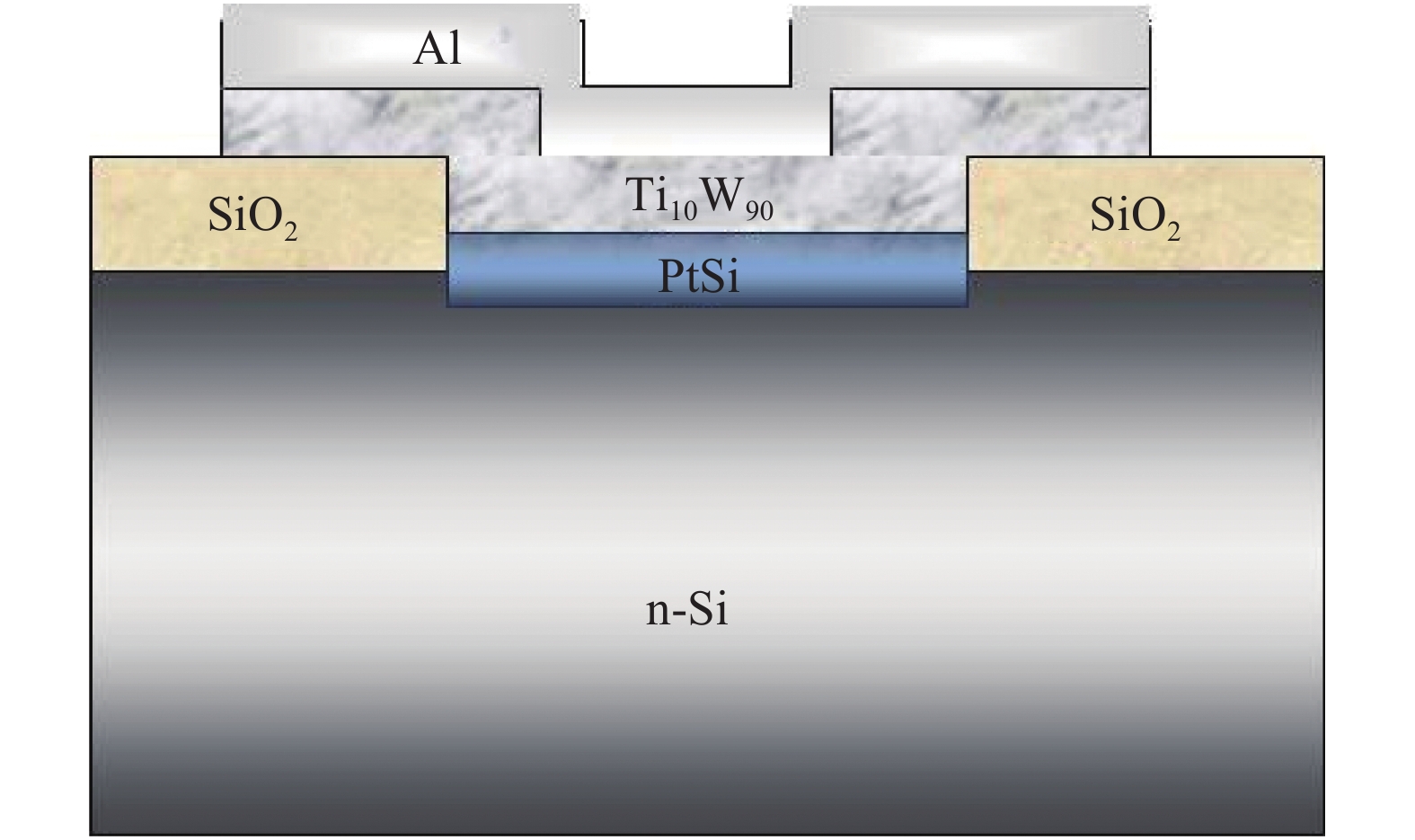
Fig. 1.
(Color online) Cross section of PtSi/n-Si (111) with diffusion barrier.
SEMICONDUCTOR DEVICES
I. M. Afandiyeva1, , ?. Altιndal2, L. K. Abdullayeva1 and A. ?. Bayramova3
Corresponding author: I. M. Afandiyeva, E-mail address: I_afandiyeva@yahoo.com
Abstract: Using the effect of the temperature on the capacitance–voltage (C–V) and conductance–voltage (G/ω–V) characteristics of PtSi/n-Si (111) Schottky diodes the profile of apparent doping concentration (NDapp), the potential difference between the Fermi energy level and the bottom of the conduction band (Vn), apparent barrier height (ΦBapp), series resistance (Rs) and the interface state density Nss have been investigated. From the temperature dependence of (C–V) it was found that these parameters are non-uniformly changed with increasing temperature in a wide temperature range of 79–360 K. The voltage and temperature dependences of apparent carrier distribution we attributed to the existence of self-assembled patches similar the quantum wells, which formed due to the process of PtSi formation on semiconductor and the presence of hexagonal voids of Si (111).
Key words: Schottky barrier diode (SBD), temperature dependence, self-assembled patches, temperature dependence, PtSi/n-Si (111), C–V characteristics, quantum wells
| [1] |
Pellegrini B . Current–voltage characteristics of silicon metallic silicide interfaces. Solid State Electron, 1975, 18(5): 417 doi: 10.1016/0038-1101(75)90043-X
|
| [2] |
Murarka S P. Silicides for VLSI application. New York: Academic Press, 1983
|
| [3] |
Sze S M. Physics of semiconductor devices. New York: John Wiley and Sons, 1981
|
| [4] |
Strikha V I. Theoretical bases of metal–semiconductor contact work. Kiev, Naukova Dumka, 1974 (in Russian)
|
| [5] |
Poate J M, Tu K N, Mayer J W. Thin films—interdiffusion and reactions. New York: Wiley-Interscience, 1978
|
| [6] |
Shaskolskaya M P. Crystallography. Moscow, Visshaya shkola, 1984
|
| [7] |
Li C P, Wang N. Metal silicide/silicon nanowires from metal vapor vacuum arc implantation. Adv Mater, 2002, 14(3): 218 doi: 10.1002/(ISSN)1521-4095
|
| [8] |
Wu W W, He J H, Cheng S L, et al. Self-assembled NiSi quantum-dot arrays on epitaxial Si0.7Ge0.3 on (001) Si. Appl Phys Lett, 2003, 83(9): 1836 doi: 10.1063/1.1605242
|
| [9] |
Chen P, Zhang J J, Feser J P, et al. Thermal transport through short-period SiGe nanodot superlattices. J Appl Phys, 2014, 115(4): 044312 doi: 10.1063/1.4863115
|
| [10] |
Lin J F, Bird J P, He Z, et al. Signatures of quantum transport in self-assembled epitaxialnickel silicide nanowires. Appl Phys Lett, 2004, 85(2): 281 doi: 10.1063/1.1769583
|
| [11] |
Stevens M, He Z, Smith D J, et al. Structure and orientation of epitaxial titanium silicide nanowires determined by electron microdiffraction. J Appl Phys, 2003, 93(9): 5670 doi: 10.1063/1.1565173
|
| [12] |
Yang W C, Ade H, Nemanich R J. Shape stability of TiSi2 islands on Si (111). J Appl Phys, 2004, 95(3): 1572 doi: 10.1063/1.1636526
|
| [13] |
Kukushkin S A. Nanoassembly films—a new method of growing epitaxial defect-free structures. Institute of Problems of Mechanical Engineering, 2010
|
| [14] |
Nogami J, Liu B Z, Katkov M V, et al. Self-assembled rare-earth silicide nanowires on Si (001). Phys Rev B, 2001, 63(23): 233305 doi: 10.1103/PhysRevB.63.233305
|
| [15] |
Balan N N, Ivashov E N, Nevsky A B. Platinum silicide as electrode material of microfabricated quantum electron tunneling transducers. 11th International Conference and Seminar on Micro/Nanotechnologies and Electron Devices, 2010: 159
|
| [16] |
Gholami S, Hajghassem H, Erfanian A R. The gaussian distribution of inhomogeneous barrier heights in PtSi/p-Si Schottky diodes. IEICE Electron Express, 2009, 6(13): 972 doi: 10.1587/elex.6.972
|
| [17] |
Gonzalez F L, Cordon M J. Enhancing near-infrared light absorption in PtSi thin films for Schottky barrier IR detectors using moth-eye surface structures. Optics Lett, 2015, 40: 1512 doi: 10.1364/OL.40.001512
|
| [18] |
Choi W, Jun D, Kim S, et al. Thermoelectric characteristics of Pt-silicide/silicon multi-layer structured p-type silicon. Energy, 2015, 82: 180 doi: 10.1016/j.energy.2015.01.024
|
| [19] |
Hsu H F, Chiang T F, Hsu H C, et al. Shape transition in the initial growth of titanium silicide clusters on Si (111). Jpn J Appl Physi, 2004, 43(7S): 4541
|
| [20] |
Nijdam A J, Gardeniers J G E, Gui C, et al. Etching pits and dislocations in Si {111}. Sens Actuators A, 2000, 86(3): 238 doi: 10.1016/S0924-4247(00)00458-1
|
| [21] |
Padma R, Lakshmi B P, Reddy V R. Capacitance–frequency (C–f) and conductance–frequency (G–f) characteristics of Ir/n-InGaN Schottky diode as a function of temperature. Superlattices Microstruct, 2013, 60: 358 doi: 10.1016/j.spmi.2013.05.014
|
| [22] |
Tataro?lu A, Güven G G, Yilmaz S, et al. Analysis of barrier height and carrier concentration of MOS capacitor using C–f and G/ω–f measurement. Gazi University Journal of Science, 2014, 27(3): 909
|
| [23] |
Soltanovich O A, Shmidt N M, Yakimov E B. Frequency and temperature dependences of capacitance–voltage characteristics of InGaN/GaN light-emitting structures with multiple quantum wells. Semiconductors, 2011, 45(2): 221 doi: 10.1134/S1063782611020205
|
| [24] |
Buzanyova E V. Microstructures of integrated electronics. Moscow, Radio i Svyaz, 1990
|
| [25] |
Tun? T, Alt?ndal ?, D?kme I, et al. Anomalous peak in the forward-bias C–V plot and temperature-dependent behavior of Au/PVA (Ni, Zn-doped)/n-Si (111) structures. J Electron Mater, 2011, 40(2): 157 doi: 10.1007/s11664-010-1440-9
|
| [26] |
Afandiyeva I M, Alt?ndal ?, Abdullayeva L K, et al. The frequency and voltage dependent electrical characteristics of AlTiW-Pd2Si/n-Si structure using I–V, C–V and G/ω–V measurements. Microelectron Eng, 2008, 85: 365 doi: 10.1016/j.mee.2007.07.010
|
| [27] |
Afandiyeva I M, Askerov S G, Abdullayeva L K, et al. The obtaining of Al-Ti10W90-Si(n) Schottky diodes and investigation of their interface surface states density. Solid State Electron, 2007, 51: 1096 doi: 10.1016/j.sse.2007.05.021
|
| [28] |
Sakurai Y, Takeda Y, Ikeda S, et al. Electrical resistivity and its thermal coefficient of TiW alloy thin films prepared by two different sputtering systems. Phys Status Solidi C, 2014, 11(9/10): 1423
|
| [29] |
Kwak J S, Kang K M, Park M J, et al. Improved thermal stability of GaN-based flip-chip light-emitting diodes with TiW-based diffusion barrier. Sci Adv Mater, 2014, 6(10): 2249 doi: 10.1166/sam.2014.2075
|
| [30] |
Afandiyeva I M, Alt?ndal ?, Abdullayeva L K. Illumination dependent electrical characteristics of PtSi/n-Si (111) schottky barrier diodes (SBDS) at room temperature. J Modern Technol Eng, 2017, 2(1): 43
|
| [31] |
Emel’yanov A M, Sobolev N A, Yakimenko A N. Capacitance–voltage characteristics of p–n structures based on (111)Si doped with erbium and oxygen. Semiconductors, 2001, 35(3): 316 doi: 10.1134/1.1356154
|
| [32] |
Chopra K, Das S. Thin film solar cells. Moskow: Plenum Press, 1986 (in Russian)
|
| [33] |
Mtangi W, Auret F D, Nyamhere C, et al. Analysis of temperature dependent I–V measurements on Pd/ZnO Schottky barrier diodes and the determination of the Richardson constant. Physica B, 2009, 404(8): 1092
|
| [34] |
Nicollian E H, Brews J R. MOS physics and technology. New York: Wiley, 1982
|
| [35] |
Afandiyeva I M, Demirezen S, Alt?ndal ?. Temperature dependence of forward and reverse bias current–voltage characteristics in Al–TiW–PtSi/nSi Schottky barrier diodes with the amorphous diffusion barrier. J Alloys Comp, 2013, 552: 423 doi: 10.1016/j.jallcom.2012.11.093
|
| [36] |
Afandiyeva I M, Alt?ndal ?, Abdullayeva L K, et al. The investigation of tunnel properties of Al-TiW-PtSi/n-Si (111) (MS) schottky barrier diodes (SBDS) in the wide temperature range. Journal of Qafqaz University, 2014, 2(2): 107
|
| [37] |
Tung R T. Electron transport at metal-semiconductor interfaces: general theory. Phys Rev B, 1992, 45(23): 13509 doi: 10.1103/PhysRevB.45.13509
|
| [38] |
Krylov P N. Physical models of thermo-processed contact metal–semiconductors. Journal of Udmurt University, 2006, 4: 125
|
| [39] |
Zhu S, Detavernier C, Van Meirhaeghe R L, et al. Electrical characteristics of CoSi2/n-Si (100) Schottky barrier contacts formed by solid state reaction. Solid State Electron, 2000, 44: 1807 doi: 10.1016/S0038-1101(00)00127-1
|
| [40] |
Werner J H, Guttler H H. Temperature dependence of Schottky barrier heights on silicon. J Appl Phys, 1993, 73: 1315 doi: 10.1063/1.353249
|
| [41] |
Blank T V, Gol’Dberg Y A. Mechanisms of current flow in metal–semiconductor ohmic contacts. Phys Technol Semicond, 2007, 7(11): 1281
|
| [42] |
Lin Y C, Lu K C, Wu W W, et al. Single crystalline PtSi nanowires, PtSi/Si/PtSi nanowire heterostructures, and nanodevice. Nano Lett, 2008, 8: 913 doi: 10.1021/nl073279r
|
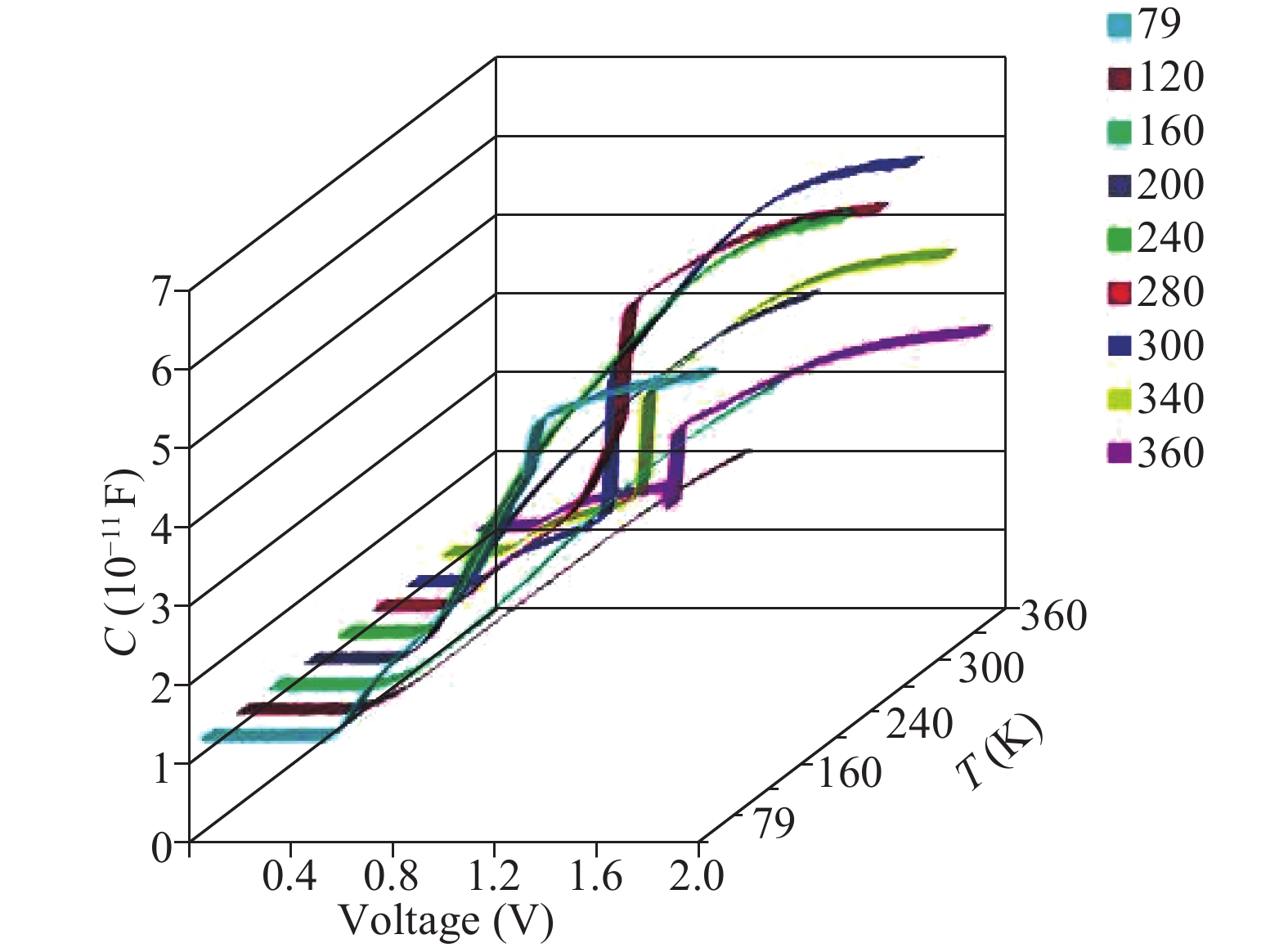

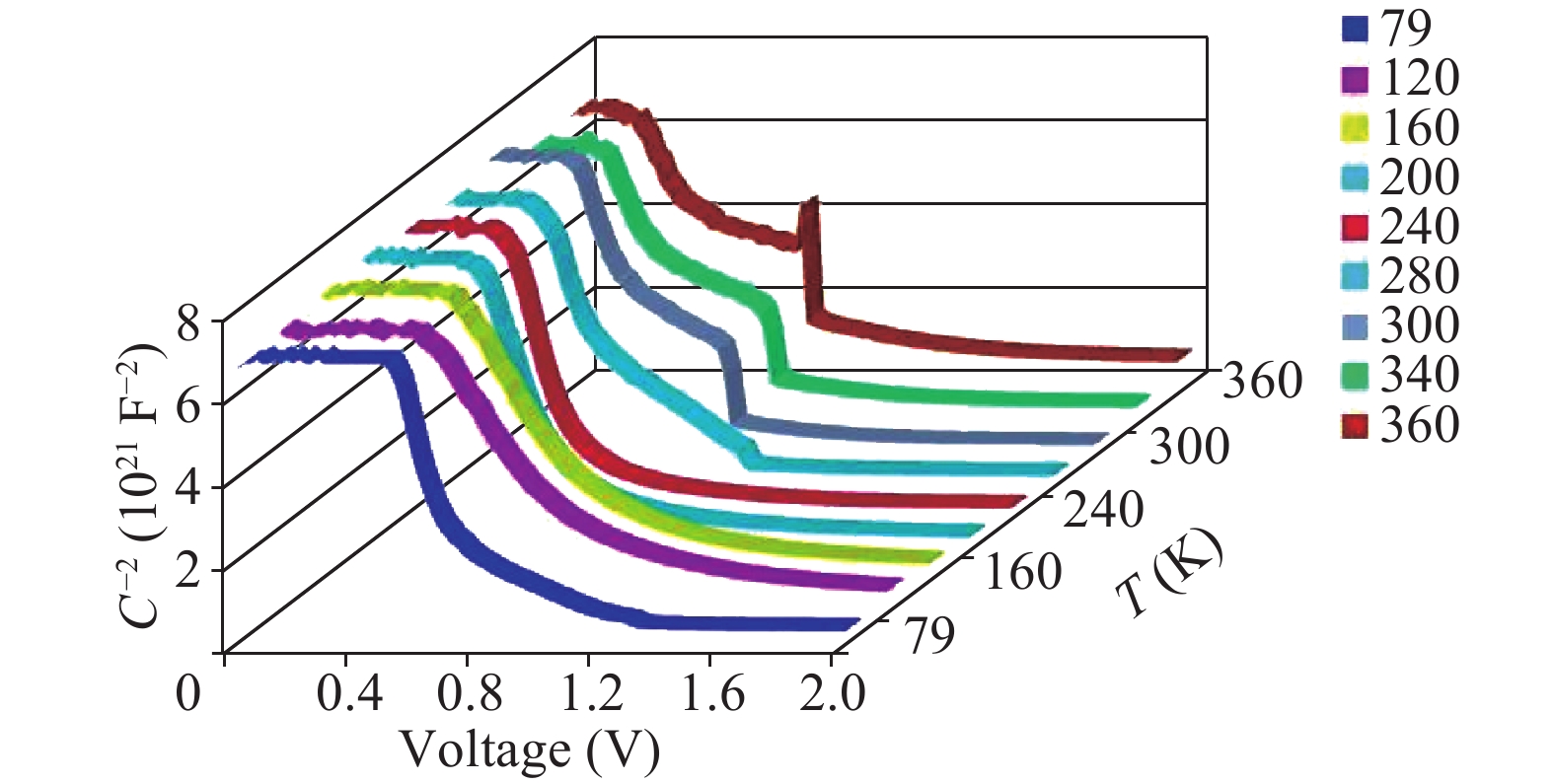
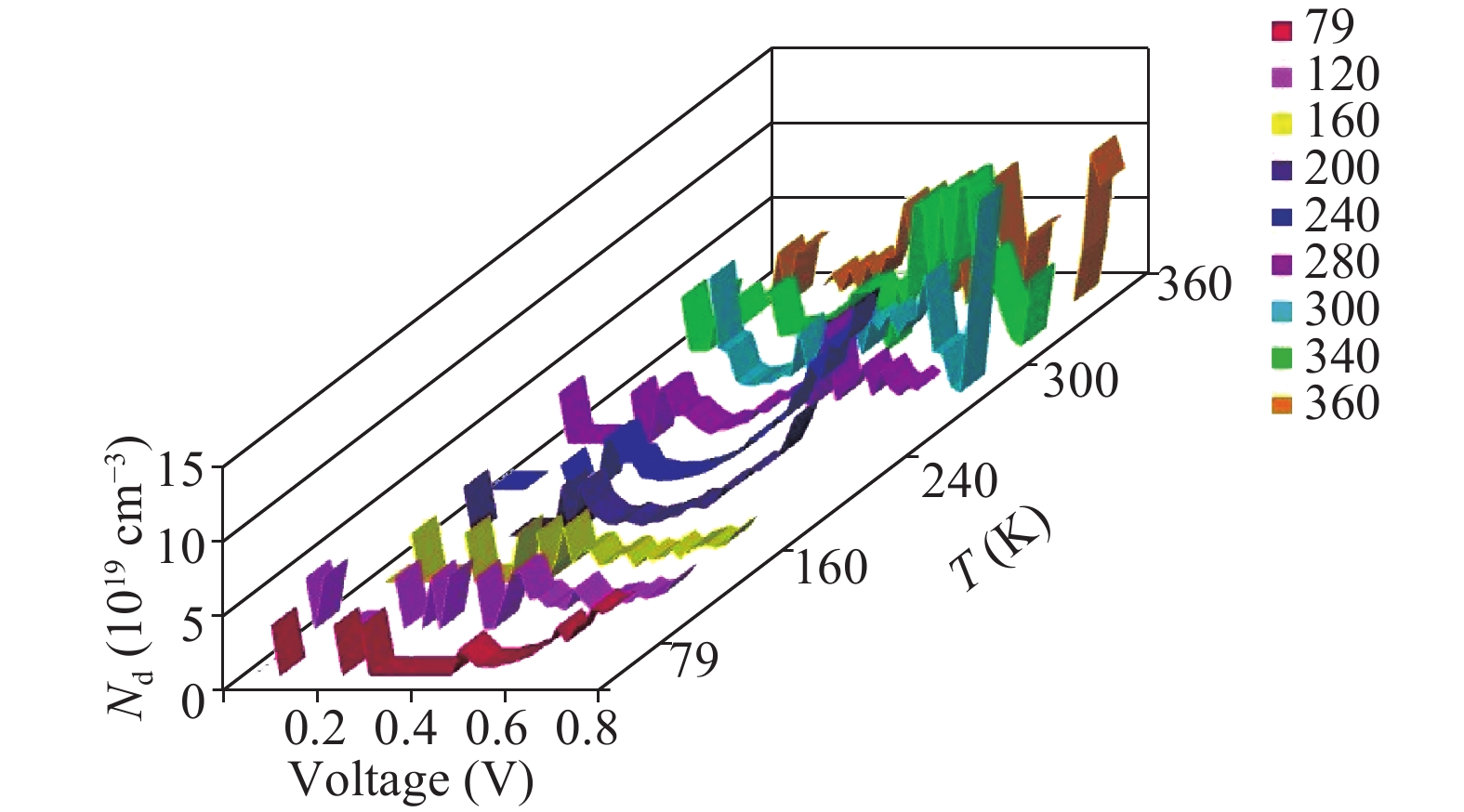
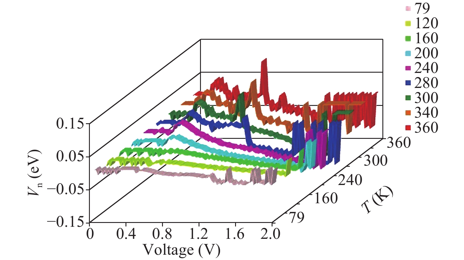
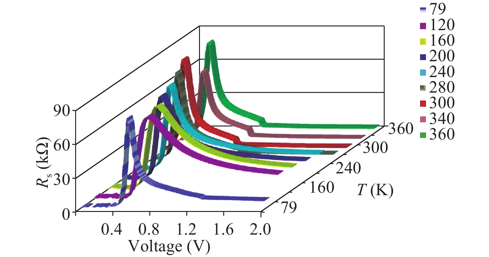
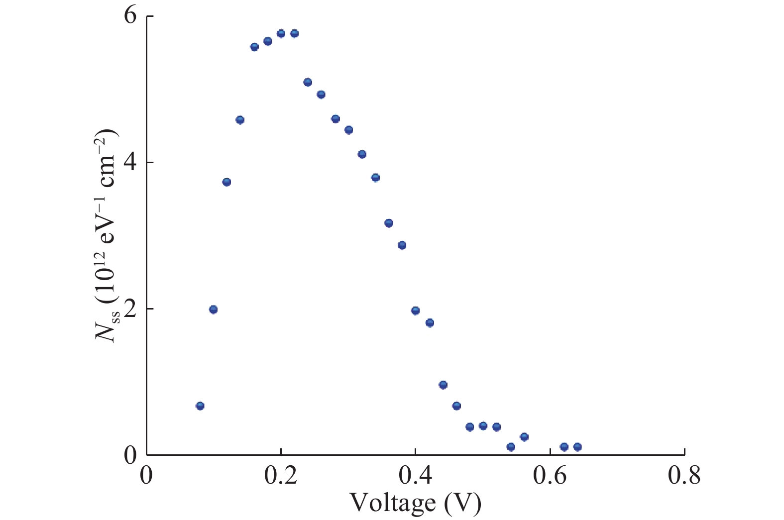
Table 1. The parameters for PtSi/n-Si (111) SBD at temperature from 79 to 360 K.
| N | T (K) | EF – Ec (5kT/q eV) | Ec – EF = Vn max (10?2 eV) | ΦB app (eV) | Rs max (Ω) | ||
| 1 | 79 | 0.039 | ?0.016 | 0.65 | 8.04 | ||
| 2 | 120 | 0.05 | ?0.017 | 0.91 | 7.28 | ||
| 3 | 160 | 0.064 | ?0.015 | 0.91 | 7.34 | ||
| 4 | 200 | 0.086 | ?0.014 | 0.52 | 7.4 | ||
| 5 | 240 | 0.1 | ?0.029 | 0.68 | 7.48 | ||
| 6 | 280 | 0.12 | ?0.033 | 0.53 | 7.9 | ||
| 7 | 300 | 0.129 | 0.056 | 0.53 | 8.19 | ||
| 8 | 340 | 0.148 | 0.066 | 0.55 | 6.3 | ||
| 9 | 360 | 0.155 | 0.101 | 0.84 | 7.98 |
 DownLoad: CSV
| [1] |
Pellegrini B . Current–voltage characteristics of silicon metallic silicide interfaces. Solid State Electron, 1975, 18(5): 417 doi: 10.1016/0038-1101(75)90043-X
|
| [2] |
Murarka S P. Silicides for VLSI application. New York: Academic Press, 1983
|
| [3] |
Sze S M. Physics of semiconductor devices. New York: John Wiley and Sons, 1981
|
| [4] |
Strikha V I. Theoretical bases of metal–semiconductor contact work. Kiev, Naukova Dumka, 1974 (in Russian)
|
| [5] |
Poate J M, Tu K N, Mayer J W. Thin films—interdiffusion and reactions. New York: Wiley-Interscience, 1978
|
| [6] |
Shaskolskaya M P. Crystallography. Moscow, Visshaya shkola, 1984
|
| [7] |
Li C P, Wang N. Metal silicide/silicon nanowires from metal vapor vacuum arc implantation. Adv Mater, 2002, 14(3): 218 doi: 10.1002/(ISSN)1521-4095
|
| [8] |
Wu W W, He J H, Cheng S L, et al. Self-assembled NiSi quantum-dot arrays on epitaxial Si0.7Ge0.3 on (001) Si. Appl Phys Lett, 2003, 83(9): 1836 doi: 10.1063/1.1605242
|
| [9] |
Chen P, Zhang J J, Feser J P, et al. Thermal transport through short-period SiGe nanodot superlattices. J Appl Phys, 2014, 115(4): 044312 doi: 10.1063/1.4863115
|
| [10] |
Lin J F, Bird J P, He Z, et al. Signatures of quantum transport in self-assembled epitaxialnickel silicide nanowires. Appl Phys Lett, 2004, 85(2): 281 doi: 10.1063/1.1769583
|
| [11] |
Stevens M, He Z, Smith D J, et al. Structure and orientation of epitaxial titanium silicide nanowires determined by electron microdiffraction. J Appl Phys, 2003, 93(9): 5670 doi: 10.1063/1.1565173
|
| [12] |
Yang W C, Ade H, Nemanich R J. Shape stability of TiSi2 islands on Si (111). J Appl Phys, 2004, 95(3): 1572 doi: 10.1063/1.1636526
|
| [13] |
Kukushkin S A. Nanoassembly films—a new method of growing epitaxial defect-free structures. Institute of Problems of Mechanical Engineering, 2010
|
| [14] |
Nogami J, Liu B Z, Katkov M V, et al. Self-assembled rare-earth silicide nanowires on Si (001). Phys Rev B, 2001, 63(23): 233305 doi: 10.1103/PhysRevB.63.233305
|
| [15] |
Balan N N, Ivashov E N, Nevsky A B. Platinum silicide as electrode material of microfabricated quantum electron tunneling transducers. 11th International Conference and Seminar on Micro/Nanotechnologies and Electron Devices, 2010: 159
|
| [16] |
Gholami S, Hajghassem H, Erfanian A R. The gaussian distribution of inhomogeneous barrier heights in PtSi/p-Si Schottky diodes. IEICE Electron Express, 2009, 6(13): 972 doi: 10.1587/elex.6.972
|
| [17] |
Gonzalez F L, Cordon M J. Enhancing near-infrared light absorption in PtSi thin films for Schottky barrier IR detectors using moth-eye surface structures. Optics Lett, 2015, 40: 1512 doi: 10.1364/OL.40.001512
|
| [18] |
Choi W, Jun D, Kim S, et al. Thermoelectric characteristics of Pt-silicide/silicon multi-layer structured p-type silicon. Energy, 2015, 82: 180 doi: 10.1016/j.energy.2015.01.024
|
| [19] |
Hsu H F, Chiang T F, Hsu H C, et al. Shape transition in the initial growth of titanium silicide clusters on Si (111). Jpn J Appl Physi, 2004, 43(7S): 4541
|
| [20] |
Nijdam A J, Gardeniers J G E, Gui C, et al. Etching pits and dislocations in Si {111}. Sens Actuators A, 2000, 86(3): 238 doi: 10.1016/S0924-4247(00)00458-1
|
| [21] |
Padma R, Lakshmi B P, Reddy V R. Capacitance–frequency (C–f) and conductance–frequency (G–f) characteristics of Ir/n-InGaN Schottky diode as a function of temperature. Superlattices Microstruct, 2013, 60: 358 doi: 10.1016/j.spmi.2013.05.014
|
| [22] |
Tataro?lu A, Güven G G, Yilmaz S, et al. Analysis of barrier height and carrier concentration of MOS capacitor using C–f and G/ω–f measurement. Gazi University Journal of Science, 2014, 27(3): 909
|
| [23] |
Soltanovich O A, Shmidt N M, Yakimov E B. Frequency and temperature dependences of capacitance–voltage characteristics of InGaN/GaN light-emitting structures with multiple quantum wells. Semiconductors, 2011, 45(2): 221 doi: 10.1134/S1063782611020205
|
| [24] |
Buzanyova E V. Microstructures of integrated electronics. Moscow, Radio i Svyaz, 1990
|
| [25] |
Tun? T, Alt?ndal ?, D?kme I, et al. Anomalous peak in the forward-bias C–V plot and temperature-dependent behavior of Au/PVA (Ni, Zn-doped)/n-Si (111) structures. J Electron Mater, 2011, 40(2): 157 doi: 10.1007/s11664-010-1440-9
|
| [26] |
Afandiyeva I M, Alt?ndal ?, Abdullayeva L K, et al. The frequency and voltage dependent electrical characteristics of AlTiW-Pd2Si/n-Si structure using I–V, C–V and G/ω–V measurements. Microelectron Eng, 2008, 85: 365 doi: 10.1016/j.mee.2007.07.010
|
| [27] |
Afandiyeva I M, Askerov S G, Abdullayeva L K, et al. The obtaining of Al-Ti10W90-Si(n) Schottky diodes and investigation of their interface surface states density. Solid State Electron, 2007, 51: 1096 doi: 10.1016/j.sse.2007.05.021
|
| [28] |
Sakurai Y, Takeda Y, Ikeda S, et al. Electrical resistivity and its thermal coefficient of TiW alloy thin films prepared by two different sputtering systems. Phys Status Solidi C, 2014, 11(9/10): 1423
|
| [29] |
Kwak J S, Kang K M, Park M J, et al. Improved thermal stability of GaN-based flip-chip light-emitting diodes with TiW-based diffusion barrier. Sci Adv Mater, 2014, 6(10): 2249 doi: 10.1166/sam.2014.2075
|
| [30] |
Afandiyeva I M, Alt?ndal ?, Abdullayeva L K. Illumination dependent electrical characteristics of PtSi/n-Si (111) schottky barrier diodes (SBDS) at room temperature. J Modern Technol Eng, 2017, 2(1): 43
|
| [31] |
Emel’yanov A M, Sobolev N A, Yakimenko A N. Capacitance–voltage characteristics of p–n structures based on (111)Si doped with erbium and oxygen. Semiconductors, 2001, 35(3): 316 doi: 10.1134/1.1356154
|
| [32] |
Chopra K, Das S. Thin film solar cells. Moskow: Plenum Press, 1986 (in Russian)
|
| [33] |
Mtangi W, Auret F D, Nyamhere C, et al. Analysis of temperature dependent I–V measurements on Pd/ZnO Schottky barrier diodes and the determination of the Richardson constant. Physica B, 2009, 404(8): 1092
|
| [34] |
Nicollian E H, Brews J R. MOS physics and technology. New York: Wiley, 1982
|
| [35] |
Afandiyeva I M, Demirezen S, Alt?ndal ?. Temperature dependence of forward and reverse bias current–voltage characteristics in Al–TiW–PtSi/nSi Schottky barrier diodes with the amorphous diffusion barrier. J Alloys Comp, 2013, 552: 423 doi: 10.1016/j.jallcom.2012.11.093
|
| [36] |
Afandiyeva I M, Alt?ndal ?, Abdullayeva L K, et al. The investigation of tunnel properties of Al-TiW-PtSi/n-Si (111) (MS) schottky barrier diodes (SBDS) in the wide temperature range. Journal of Qafqaz University, 2014, 2(2): 107
|
| [37] |
Tung R T. Electron transport at metal-semiconductor interfaces: general theory. Phys Rev B, 1992, 45(23): 13509 doi: 10.1103/PhysRevB.45.13509
|
| [38] |
Krylov P N. Physical models of thermo-processed contact metal–semiconductors. Journal of Udmurt University, 2006, 4: 125
|
| [39] |
Zhu S, Detavernier C, Van Meirhaeghe R L, et al. Electrical characteristics of CoSi2/n-Si (100) Schottky barrier contacts formed by solid state reaction. Solid State Electron, 2000, 44: 1807 doi: 10.1016/S0038-1101(00)00127-1
|
| [40] |
Werner J H, Guttler H H. Temperature dependence of Schottky barrier heights on silicon. J Appl Phys, 1993, 73: 1315 doi: 10.1063/1.353249
|
| [41] |
Blank T V, Gol’Dberg Y A. Mechanisms of current flow in metal–semiconductor ohmic contacts. Phys Technol Semicond, 2007, 7(11): 1281
|
| [42] |
Lin Y C, Lu K C, Wu W W, et al. Single crystalline PtSi nanowires, PtSi/Si/PtSi nanowire heterostructures, and nanodevice. Nano Lett, 2008, 8: 913 doi: 10.1021/nl073279r
|


Article views: 4252 Times PDF downloads: 43 Times Cited by: 0 Times
Received: 05 October 2017 Revised: 05 December 2017 Online: Accepted Manuscript: 19 January 2018Uncorrected proof: 24 January 2018Published: 01 May 2018
| Citation: |
I. M. Afandiyeva, ?. Altιndal, L. K. Abdullayeva, A. ?. Bayramova. Self-assembled patches in PtSi/n-Si (111) diodes[J]. Journal of Semiconductors, 2018, 39(5): 054002. doi: 10.1088/1674-4926/39/5/054002
****
I. M. Afandiyeva, ?. Altιndal, L. K. Abdullayeva, A. ?. Bayramova. Self-assembled patches in PtSi/n-Si (111) diodes[J]. J. Semicond., 2018, 39(5): 054002. doi: 10.1088/1674-4926/39/5/054002.

|
| [1] |
Pellegrini B . Current–voltage characteristics of silicon metallic silicide interfaces. Solid State Electron, 1975, 18(5): 417 doi: 10.1016/0038-1101(75)90043-X
|
| [2] |
Murarka S P. Silicides for VLSI application. New York: Academic Press, 1983
|
| [3] |
Sze S M. Physics of semiconductor devices. New York: John Wiley and Sons, 1981
|
| [4] |
Strikha V I. Theoretical bases of metal–semiconductor contact work. Kiev, Naukova Dumka, 1974 (in Russian)
|
| [5] |
Poate J M, Tu K N, Mayer J W. Thin films—interdiffusion and reactions. New York: Wiley-Interscience, 1978
|
| [6] |
Shaskolskaya M P. Crystallography. Moscow, Visshaya shkola, 1984
|
| [7] |
Li C P, Wang N. Metal silicide/silicon nanowires from metal vapor vacuum arc implantation. Adv Mater, 2002, 14(3): 218 doi: 10.1002/(ISSN)1521-4095
|
| [8] |
Wu W W, He J H, Cheng S L, et al. Self-assembled NiSi quantum-dot arrays on epitaxial Si0.7Ge0.3 on (001) Si. Appl Phys Lett, 2003, 83(9): 1836 doi: 10.1063/1.1605242
|
| [9] |
Chen P, Zhang J J, Feser J P, et al. Thermal transport through short-period SiGe nanodot superlattices. J Appl Phys, 2014, 115(4): 044312 doi: 10.1063/1.4863115
|
| [10] |
Lin J F, Bird J P, He Z, et al. Signatures of quantum transport in self-assembled epitaxialnickel silicide nanowires. Appl Phys Lett, 2004, 85(2): 281 doi: 10.1063/1.1769583
|
| [11] |
Stevens M, He Z, Smith D J, et al. Structure and orientation of epitaxial titanium silicide nanowires determined by electron microdiffraction. J Appl Phys, 2003, 93(9): 5670 doi: 10.1063/1.1565173
|
| [12] |
Yang W C, Ade H, Nemanich R J. Shape stability of TiSi2 islands on Si (111). J Appl Phys, 2004, 95(3): 1572 doi: 10.1063/1.1636526
|
| [13] |
Kukushkin S A. Nanoassembly films—a new method of growing epitaxial defect-free structures. Institute of Problems of Mechanical Engineering, 2010
|
| [14] |
Nogami J, Liu B Z, Katkov M V, et al. Self-assembled rare-earth silicide nanowires on Si (001). Phys Rev B, 2001, 63(23): 233305 doi: 10.1103/PhysRevB.63.233305
|
| [15] |
Balan N N, Ivashov E N, Nevsky A B. Platinum silicide as electrode material of microfabricated quantum electron tunneling transducers. 11th International Conference and Seminar on Micro/Nanotechnologies and Electron Devices, 2010: 159
|
| [16] |
Gholami S, Hajghassem H, Erfanian A R. The gaussian distribution of inhomogeneous barrier heights in PtSi/p-Si Schottky diodes. IEICE Electron Express, 2009, 6(13): 972 doi: 10.1587/elex.6.972
|
| [17] |
Gonzalez F L, Cordon M J. Enhancing near-infrared light absorption in PtSi thin films for Schottky barrier IR detectors using moth-eye surface structures. Optics Lett, 2015, 40: 1512 doi: 10.1364/OL.40.001512
|
| [18] |
Choi W, Jun D, Kim S, et al. Thermoelectric characteristics of Pt-silicide/silicon multi-layer structured p-type silicon. Energy, 2015, 82: 180 doi: 10.1016/j.energy.2015.01.024
|
| [19] |
Hsu H F, Chiang T F, Hsu H C, et al. Shape transition in the initial growth of titanium silicide clusters on Si (111). Jpn J Appl Physi, 2004, 43(7S): 4541
|
| [20] |
Nijdam A J, Gardeniers J G E, Gui C, et al. Etching pits and dislocations in Si {111}. Sens Actuators A, 2000, 86(3): 238 doi: 10.1016/S0924-4247(00)00458-1
|
| [21] |
Padma R, Lakshmi B P, Reddy V R. Capacitance–frequency (C–f) and conductance–frequency (G–f) characteristics of Ir/n-InGaN Schottky diode as a function of temperature. Superlattices Microstruct, 2013, 60: 358 doi: 10.1016/j.spmi.2013.05.014
|
| [22] |
Tataro?lu A, Güven G G, Yilmaz S, et al. Analysis of barrier height and carrier concentration of MOS capacitor using C–f and G/ω–f measurement. Gazi University Journal of Science, 2014, 27(3): 909
|
| [23] |
Soltanovich O A, Shmidt N M, Yakimov E B. Frequency and temperature dependences of capacitance–voltage characteristics of InGaN/GaN light-emitting structures with multiple quantum wells. Semiconductors, 2011, 45(2): 221 doi: 10.1134/S1063782611020205
|
| [24] |
Buzanyova E V. Microstructures of integrated electronics. Moscow, Radio i Svyaz, 1990
|
| [25] |
Tun? T, Alt?ndal ?, D?kme I, et al. Anomalous peak in the forward-bias C–V plot and temperature-dependent behavior of Au/PVA (Ni, Zn-doped)/n-Si (111) structures. J Electron Mater, 2011, 40(2): 157 doi: 10.1007/s11664-010-1440-9
|
| [26] |
Afandiyeva I M, Alt?ndal ?, Abdullayeva L K, et al. The frequency and voltage dependent electrical characteristics of AlTiW-Pd2Si/n-Si structure using I–V, C–V and G/ω–V measurements. Microelectron Eng, 2008, 85: 365 doi: 10.1016/j.mee.2007.07.010
|
| [27] |
Afandiyeva I M, Askerov S G, Abdullayeva L K, et al. The obtaining of Al-Ti10W90-Si(n) Schottky diodes and investigation of their interface surface states density. Solid State Electron, 2007, 51: 1096 doi: 10.1016/j.sse.2007.05.021
|
| [28] |
Sakurai Y, Takeda Y, Ikeda S, et al. Electrical resistivity and its thermal coefficient of TiW alloy thin films prepared by two different sputtering systems. Phys Status Solidi C, 2014, 11(9/10): 1423
|
| [29] |
Kwak J S, Kang K M, Park M J, et al. Improved thermal stability of GaN-based flip-chip light-emitting diodes with TiW-based diffusion barrier. Sci Adv Mater, 2014, 6(10): 2249 doi: 10.1166/sam.2014.2075
|
| [30] |
Afandiyeva I M, Alt?ndal ?, Abdullayeva L K. Illumination dependent electrical characteristics of PtSi/n-Si (111) schottky barrier diodes (SBDS) at room temperature. J Modern Technol Eng, 2017, 2(1): 43
|
| [31] |
Emel’yanov A M, Sobolev N A, Yakimenko A N. Capacitance–voltage characteristics of p–n structures based on (111)Si doped with erbium and oxygen. Semiconductors, 2001, 35(3): 316 doi: 10.1134/1.1356154
|
| [32] |
Chopra K, Das S. Thin film solar cells. Moskow: Plenum Press, 1986 (in Russian)
|
| [33] |
Mtangi W, Auret F D, Nyamhere C, et al. Analysis of temperature dependent I–V measurements on Pd/ZnO Schottky barrier diodes and the determination of the Richardson constant. Physica B, 2009, 404(8): 1092
|
| [34] |
Nicollian E H, Brews J R. MOS physics and technology. New York: Wiley, 1982
|
| [35] |
Afandiyeva I M, Demirezen S, Alt?ndal ?. Temperature dependence of forward and reverse bias current–voltage characteristics in Al–TiW–PtSi/nSi Schottky barrier diodes with the amorphous diffusion barrier. J Alloys Comp, 2013, 552: 423 doi: 10.1016/j.jallcom.2012.11.093
|
| [36] |
Afandiyeva I M, Alt?ndal ?, Abdullayeva L K, et al. The investigation of tunnel properties of Al-TiW-PtSi/n-Si (111) (MS) schottky barrier diodes (SBDS) in the wide temperature range. Journal of Qafqaz University, 2014, 2(2): 107
|
| [37] |
Tung R T. Electron transport at metal-semiconductor interfaces: general theory. Phys Rev B, 1992, 45(23): 13509 doi: 10.1103/PhysRevB.45.13509
|
| [38] |
Krylov P N. Physical models of thermo-processed contact metal–semiconductors. Journal of Udmurt University, 2006, 4: 125
|
| [39] |
Zhu S, Detavernier C, Van Meirhaeghe R L, et al. Electrical characteristics of CoSi2/n-Si (100) Schottky barrier contacts formed by solid state reaction. Solid State Electron, 2000, 44: 1807 doi: 10.1016/S0038-1101(00)00127-1
|
| [40] |
Werner J H, Guttler H H. Temperature dependence of Schottky barrier heights on silicon. J Appl Phys, 1993, 73: 1315 doi: 10.1063/1.353249
|
| [41] |
Blank T V, Gol’Dberg Y A. Mechanisms of current flow in metal–semiconductor ohmic contacts. Phys Technol Semicond, 2007, 7(11): 1281
|
| [42] |
Lin Y C, Lu K C, Wu W W, et al. Single crystalline PtSi nanowires, PtSi/Si/PtSi nanowire heterostructures, and nanodevice. Nano Lett, 2008, 8: 913 doi: 10.1021/nl073279r
|

 WeChat ID
Journal of Semiconductors © 2017 All Rights Reserved 京ICP備05085259號-2