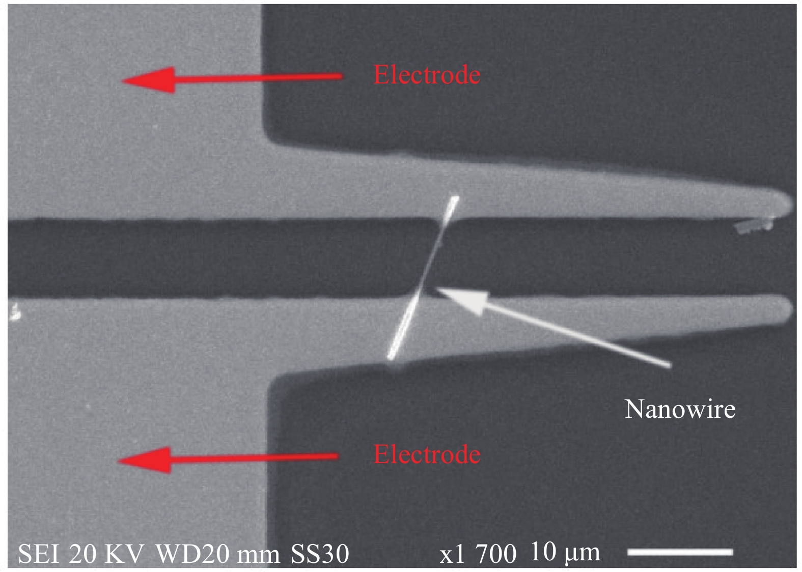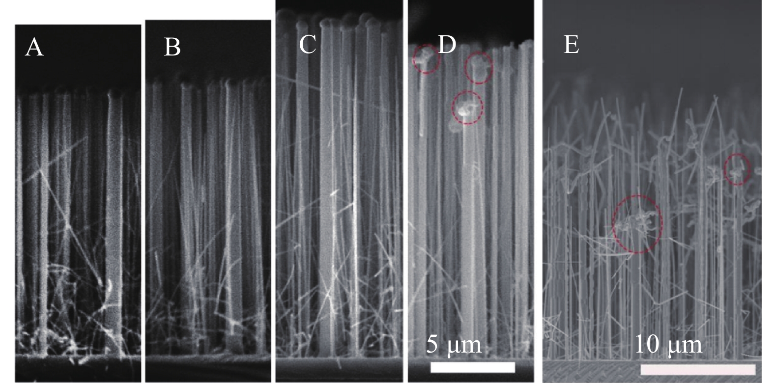
Fig. 1.
The SEM image of all the samples. The growth parameters of each sample are shown in Table 1.
SEMICONDUCTOR MATERIALS
Bang Li, Xin Yan, Xia Zhang and Xiaomin Ren
Corresponding author: Bang Li, libang@bupt.edu.cn
Abstract: The growth of p-type GaAs nanowires (NWs) on GaAs (111) B substrates by metal-organic chemical vapor deposition (MOCVD) has been systematically investigated as a function of diethyl zinc (DEZn) flow. The growth rate of GaAs NWs was slightly improved by Zn-doping and kink is observed under high DEZn flow. In addition, the I–V curves of GaAs NWs has been measured and the p-type dope concentration under the II/III ratio of 0.013 and 0.038 approximated to 1019–1020 cm?3.
| [1] |
Dai X, Zhang S, Wang Z, et al. GaAs/AlGaAs nanowire photodetector. Nano Lett, 2014, 14(5): 2688 doi: 10.1021/nl5006004
|
| [2] |
Tsakalakos L, Balch J, Fronheiser J, et al. Silicon nanowire solar cells. Appl Phys Lett, 2007, 91(23): 233117 doi: 10.1063/1.2821113
|
| [3] |
Piccione B, Cho C, Vugt L K, et al. All-optical active switching in individual semiconductor nanowires. Nat Nanotechnol, 2012, 7: 640 doi: 10.1038/nnano.2012.144
|
| [4] |
Pan C, Dong L, Zhu G, et al. High-resolution electroluminescent imaging of pressure distribution using a piezoelectric nanowire LED array. Nat Photonics, 2013, 7(9): 752 doi: 10.1038/nphoton.2013.191
|
| [5] |
Hoa N D, Le D T T, Tam P D, et al. On-chip fabrication of SnO2-nanowire gas sensor: The effect of growth time on sensor performance. Sens Actuator B, 2010, 146(1): 361 doi: 10.1016/j.snb.2010.02.054
|
| [6] |
Vitiello M S, Coquillat D, Viti L, et al. Room-temperature terahertz detectors based on semiconductor nanowire field-effect transistors. Nano Lett, 2011, 12(1): 96
|
| [7] |
Patolsky F, Zheng G, Lieber C M. Nanowire sensors for medicine and the life sciences. Future Medicine, 2006, 1(1): 51
|
| [8] |
Haraguchi K, Katsuyama T, Hiruma K, et al. GaAs p‐n junction formed in quantum wire crystals. Appl Phys Lett, 1992, 60(6): 745 doi: 10.1063/1.106556
|
| [9] |
Wagner R S, Ellis W C. Vapor-Liquid-Solid mechanism of single crystal growth. Appl Phys Lett, 1964, 4(5): 89 doi: 10.1063/1.1753975
|
| [10] |
Li H Y, Wunnicke O, Borgstr?m M T, et al. Remote p-doping of InAs nanowires. Nano Lett, 2007, 7(5): 1144 doi: 10.1021/nl0627487
|
| [11] |
Franke D, Reier F W, Grote N. Post-growth Zn diffusion into InGaAs/InP in a LP-MOVPE reactor. J Cryst Growth, 1998, 195(1–4): 112 doi: 10.1016/S0022-0248(98)00681-2
|
| [12] |
Stichtenoth D, Wegener K, Gutsche C, et al. P-type doping of GaAs nanowires. Appl Phys Lett, 2008, 92(16): 163107 doi: 10.1063/1.2912129
|
| [13] |
Gutsche C, Niepelt R, Gnauck M, et al. Direct determination of minority carrier diffusion lengths at axial GaAs nanowire p–n junctions. Nano Lett, 2012, 12(3): 1453 doi: 10.1021/nl204126n
|
| [14] |
Chang C C, Chi C Y, Yao M, et al. Electrical and optical characterization of surface passivation in GaAs nanowires. Nano Lett, 2012, 12(9): 4484 doi: 10.1021/nl301391h
|
| [15] |
Sager D, Gutsche C, Prost W, et al. Recombination dynamics in single GaAs-nanowires with an axial heterojunction: n-versus p-doped areas. J Appl Phys, 2013, 113(17): 174303 doi: 10.1063/1.4803488
|
| [16] |
Borgstr?m M T, Norberg E, Wickert P, et al. Precursor evaluation for in situ InP nanowire doping. Nanotechnology, 2008, 19(44): 445602 doi: 10.1088/0957-4484/19/44/445602
|
| [17] |
Gutsche C, Lysov A, Regolin I, et al. n-type doping of vapor–liquid–solid grown GaAs nanowires. Nanoscale Res Lett, 2011, 6(1): 65
|
| [18] |
Salehzadeh O, Kavanagh K L, Watkins S P. Controlled axial and radial Te-doping of GaAs nanowires. J Appl Phys, 2012, 112(5): 054324 doi: 10.1063/1.4751988
|
| [19] |
Joyce H J, Docherty C J, Gao Q, et al. Electronic properties of GaAs, InAs and InP nanowires studied by terahertz spectroscopy. Nanotechnology, 2013, 24(21): 214006 doi: 10.1088/0957-4484/24/21/214006
|
| [20] |
Boland J L, Conesa-Boj S, Parkinson P, et al. Modulation doping of GaAs/AlGaAs core–shell nanowires with effective defect passivation and high electron mobility. Nano Lett, 2015, 15(2): 1336 doi: 10.1021/nl504566t
|
| [21] |
Sladek K, Klinger V, Wensorra J, et al. MOVPE of n-doped GaAs and modulation doped GaAs/AlGaAs nanowires. J Cryst Growth, 2010, 312(5): 635 doi: 10.1016/j.jcrysgro.2009.11.026
|
| [22] |
Sourribes M J L, Isakov I, Panfilova M, et al. Minimization of the contact resistance between InAs nanowires and metallic contacts. Nanotechnology, 2013, 24(4): 045703 doi: 10.1088/0957-4484/24/4/045703
|
| [23] |
Gutsche C, Regolin I, Blekker K, et al. Controllable p-type doping of GaAs nanowires during vapor-liquid-solid growth. J Appl Phys, 2009, 105(2): 024305 doi: 10.1063/1.3065536
|
| [24] |
Ketterer B, Uccelli E, i Morral A F. Mobility and carrier density in p-type GaAs nanowires measured by transmission Raman spectroscopy. Nanoscale, 2012, 4(5): 1789 doi: 10.1039/c2nr11910b
|
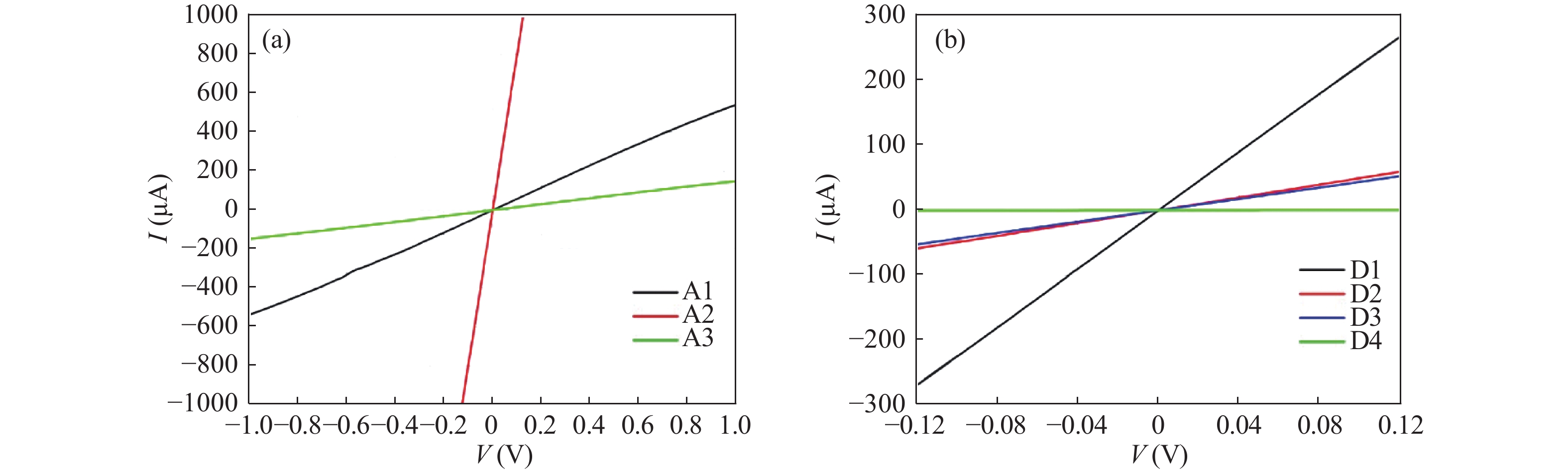
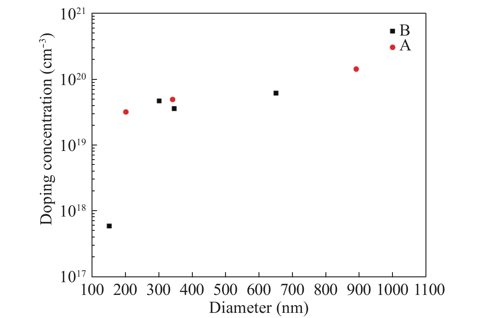
Table 1. The growth parameters of all samples.
| Sample | DEZn
flow (sccm) |
AsH3 flow (sccm) |
TMGa
flow (sccm) |
II/III ratio | Growth
temperature (°C) |
Growth
time (s) |
Height
(μm) |
| A | 5 | 100 | 14.4 | 0.013 | 490 | 2000 | 15.5 |
| B | 10 | 100 | 14.4 | 0.025 | 490 | 2000 | 16.1 |
| C | 12.5 | 100 | 14.4 | 0.031 | 490 | 2000 | 20.0 |
| D | 15 | 100 | 14.4 | 0.038 | 490 | 2000 | 17–18 |
| E | 20 | 100 | 14.4 | 0.05 | 490 | 2000 | – |
 DownLoad: CSV
Table 2. Morphology parameters and estimation resistance of these measured GaAs NWs.
| Sample | Diameter (nm) | Length (μm) | Resistance (Ω) | ||
| A1 | 340 | 6.59 | 1700 | ||
| A2 | 890 | 5.9 | 120 | ||
| A3 | 200 | 6.47 | 6500 | ||
| D1 | 650 | 7.27 | 440 | ||
| D2 | 345 | 6.68 | 2020 | ||
| D3 | 300 | 5.88 | 2290 | ||
| D4 | 150 | 6.5 | 430 000 |
DownLoad: CSV
| [1] |
Dai X, Zhang S, Wang Z, et al. GaAs/AlGaAs nanowire photodetector. Nano Lett, 2014, 14(5): 2688 doi: 10.1021/nl5006004
|
| [2] |
Tsakalakos L, Balch J, Fronheiser J, et al. Silicon nanowire solar cells. Appl Phys Lett, 2007, 91(23): 233117 doi: 10.1063/1.2821113
|
| [3] |
Piccione B, Cho C, Vugt L K, et al. All-optical active switching in individual semiconductor nanowires. Nat Nanotechnol, 2012, 7: 640 doi: 10.1038/nnano.2012.144
|
| [4] |
Pan C, Dong L, Zhu G, et al. High-resolution electroluminescent imaging of pressure distribution using a piezoelectric nanowire LED array. Nat Photonics, 2013, 7(9): 752 doi: 10.1038/nphoton.2013.191
|
| [5] |
Hoa N D, Le D T T, Tam P D, et al. On-chip fabrication of SnO2-nanowire gas sensor: The effect of growth time on sensor performance. Sens Actuator B, 2010, 146(1): 361 doi: 10.1016/j.snb.2010.02.054
|
| [6] |
Vitiello M S, Coquillat D, Viti L, et al. Room-temperature terahertz detectors based on semiconductor nanowire field-effect transistors. Nano Lett, 2011, 12(1): 96
|
| [7] |
Patolsky F, Zheng G, Lieber C M. Nanowire sensors for medicine and the life sciences. Future Medicine, 2006, 1(1): 51
|
| [8] |
Haraguchi K, Katsuyama T, Hiruma K, et al. GaAs p‐n junction formed in quantum wire crystals. Appl Phys Lett, 1992, 60(6): 745 doi: 10.1063/1.106556
|
| [9] |
Wagner R S, Ellis W C. Vapor-Liquid-Solid mechanism of single crystal growth. Appl Phys Lett, 1964, 4(5): 89 doi: 10.1063/1.1753975
|
| [10] |
Li H Y, Wunnicke O, Borgstr?m M T, et al. Remote p-doping of InAs nanowires. Nano Lett, 2007, 7(5): 1144 doi: 10.1021/nl0627487
|
| [11] |
Franke D, Reier F W, Grote N. Post-growth Zn diffusion into InGaAs/InP in a LP-MOVPE reactor. J Cryst Growth, 1998, 195(1–4): 112 doi: 10.1016/S0022-0248(98)00681-2
|
| [12] |
Stichtenoth D, Wegener K, Gutsche C, et al. P-type doping of GaAs nanowires. Appl Phys Lett, 2008, 92(16): 163107 doi: 10.1063/1.2912129
|
| [13] |
Gutsche C, Niepelt R, Gnauck M, et al. Direct determination of minority carrier diffusion lengths at axial GaAs nanowire p–n junctions. Nano Lett, 2012, 12(3): 1453 doi: 10.1021/nl204126n
|
| [14] |
Chang C C, Chi C Y, Yao M, et al. Electrical and optical characterization of surface passivation in GaAs nanowires. Nano Lett, 2012, 12(9): 4484 doi: 10.1021/nl301391h
|
| [15] |
Sager D, Gutsche C, Prost W, et al. Recombination dynamics in single GaAs-nanowires with an axial heterojunction: n-versus p-doped areas. J Appl Phys, 2013, 113(17): 174303 doi: 10.1063/1.4803488
|
| [16] |
Borgstr?m M T, Norberg E, Wickert P, et al. Precursor evaluation for in situ InP nanowire doping. Nanotechnology, 2008, 19(44): 445602 doi: 10.1088/0957-4484/19/44/445602
|
| [17] |
Gutsche C, Lysov A, Regolin I, et al. n-type doping of vapor–liquid–solid grown GaAs nanowires. Nanoscale Res Lett, 2011, 6(1): 65
|
| [18] |
Salehzadeh O, Kavanagh K L, Watkins S P. Controlled axial and radial Te-doping of GaAs nanowires. J Appl Phys, 2012, 112(5): 054324 doi: 10.1063/1.4751988
|
| [19] |
Joyce H J, Docherty C J, Gao Q, et al. Electronic properties of GaAs, InAs and InP nanowires studied by terahertz spectroscopy. Nanotechnology, 2013, 24(21): 214006 doi: 10.1088/0957-4484/24/21/214006
|
| [20] |
Boland J L, Conesa-Boj S, Parkinson P, et al. Modulation doping of GaAs/AlGaAs core–shell nanowires with effective defect passivation and high electron mobility. Nano Lett, 2015, 15(2): 1336 doi: 10.1021/nl504566t
|
| [21] |
Sladek K, Klinger V, Wensorra J, et al. MOVPE of n-doped GaAs and modulation doped GaAs/AlGaAs nanowires. J Cryst Growth, 2010, 312(5): 635 doi: 10.1016/j.jcrysgro.2009.11.026
|
| [22] |
Sourribes M J L, Isakov I, Panfilova M, et al. Minimization of the contact resistance between InAs nanowires and metallic contacts. Nanotechnology, 2013, 24(4): 045703 doi: 10.1088/0957-4484/24/4/045703
|
| [23] |
Gutsche C, Regolin I, Blekker K, et al. Controllable p-type doping of GaAs nanowires during vapor-liquid-solid growth. J Appl Phys, 2009, 105(2): 024305 doi: 10.1063/1.3065536
|
| [24] |
Ketterer B, Uccelli E, i Morral A F. Mobility and carrier density in p-type GaAs nanowires measured by transmission Raman spectroscopy. Nanoscale, 2012, 4(5): 1789 doi: 10.1039/c2nr11910b
|


Article views: 3863 Times PDF downloads: 46 Times Cited by: 0 Times
Received: 25 September 2017 Revised: 12 December 2017 Online: Uncorrected proof: 25 January 2018Accepted Manuscript: 18 April 2018Published: 01 May 2018
| Citation: |
Bang Li, Xin Yan, Xia Zhang, Xiaomin Ren. Growth and characteristics of p-type doped GaAs nanowire[J]. Journal of Semiconductors, 2018, 39(5): 053004. doi: 10.1088/1674-4926/39/5/053004
****
B Li, X Yan, X Zhang, X M Ren. Growth and characteristics of p-type doped GaAs nanowire[J]. J. Semicond., 2018, 39(5): 053004. doi: 10.1088/1674-4926/39/5/053004.

|
Project supported by the National Natural Science Foundation of China (Nos. 61376019, 61504010, 61774021) and the Fund of State Key Laboratory of Information Photonics and Optical Communications (Beijing University of Posts and Telecommunications), China (Nos. IPOC2017ZT02, IPOC2017ZZ01).
| [1] |
Dai X, Zhang S, Wang Z, et al. GaAs/AlGaAs nanowire photodetector. Nano Lett, 2014, 14(5): 2688 doi: 10.1021/nl5006004
|
| [2] |
Tsakalakos L, Balch J, Fronheiser J, et al. Silicon nanowire solar cells. Appl Phys Lett, 2007, 91(23): 233117 doi: 10.1063/1.2821113
|
| [3] |
Piccione B, Cho C, Vugt L K, et al. All-optical active switching in individual semiconductor nanowires. Nat Nanotechnol, 2012, 7: 640 doi: 10.1038/nnano.2012.144
|
| [4] |
Pan C, Dong L, Zhu G, et al. High-resolution electroluminescent imaging of pressure distribution using a piezoelectric nanowire LED array. Nat Photonics, 2013, 7(9): 752 doi: 10.1038/nphoton.2013.191
|
| [5] |
Hoa N D, Le D T T, Tam P D, et al. On-chip fabrication of SnO2-nanowire gas sensor: The effect of growth time on sensor performance. Sens Actuator B, 2010, 146(1): 361 doi: 10.1016/j.snb.2010.02.054
|
| [6] |
Vitiello M S, Coquillat D, Viti L, et al. Room-temperature terahertz detectors based on semiconductor nanowire field-effect transistors. Nano Lett, 2011, 12(1): 96
|
| [7] |
Patolsky F, Zheng G, Lieber C M. Nanowire sensors for medicine and the life sciences. Future Medicine, 2006, 1(1): 51
|
| [8] |
Haraguchi K, Katsuyama T, Hiruma K, et al. GaAs p‐n junction formed in quantum wire crystals. Appl Phys Lett, 1992, 60(6): 745 doi: 10.1063/1.106556
|
| [9] |
Wagner R S, Ellis W C. Vapor-Liquid-Solid mechanism of single crystal growth. Appl Phys Lett, 1964, 4(5): 89 doi: 10.1063/1.1753975
|
| [10] |
Li H Y, Wunnicke O, Borgstr?m M T, et al. Remote p-doping of InAs nanowires. Nano Lett, 2007, 7(5): 1144 doi: 10.1021/nl0627487
|
| [11] |
Franke D, Reier F W, Grote N. Post-growth Zn diffusion into InGaAs/InP in a LP-MOVPE reactor. J Cryst Growth, 1998, 195(1–4): 112 doi: 10.1016/S0022-0248(98)00681-2
|
| [12] |
Stichtenoth D, Wegener K, Gutsche C, et al. P-type doping of GaAs nanowires. Appl Phys Lett, 2008, 92(16): 163107 doi: 10.1063/1.2912129
|
| [13] |
Gutsche C, Niepelt R, Gnauck M, et al. Direct determination of minority carrier diffusion lengths at axial GaAs nanowire p–n junctions. Nano Lett, 2012, 12(3): 1453 doi: 10.1021/nl204126n
|
| [14] |
Chang C C, Chi C Y, Yao M, et al. Electrical and optical characterization of surface passivation in GaAs nanowires. Nano Lett, 2012, 12(9): 4484 doi: 10.1021/nl301391h
|
| [15] |
Sager D, Gutsche C, Prost W, et al. Recombination dynamics in single GaAs-nanowires with an axial heterojunction: n-versus p-doped areas. J Appl Phys, 2013, 113(17): 174303 doi: 10.1063/1.4803488
|
| [16] |
Borgstr?m M T, Norberg E, Wickert P, et al. Precursor evaluation for in situ InP nanowire doping. Nanotechnology, 2008, 19(44): 445602 doi: 10.1088/0957-4484/19/44/445602
|
| [17] |
Gutsche C, Lysov A, Regolin I, et al. n-type doping of vapor–liquid–solid grown GaAs nanowires. Nanoscale Res Lett, 2011, 6(1): 65
|
| [18] |
Salehzadeh O, Kavanagh K L, Watkins S P. Controlled axial and radial Te-doping of GaAs nanowires. J Appl Phys, 2012, 112(5): 054324 doi: 10.1063/1.4751988
|
| [19] |
Joyce H J, Docherty C J, Gao Q, et al. Electronic properties of GaAs, InAs and InP nanowires studied by terahertz spectroscopy. Nanotechnology, 2013, 24(21): 214006 doi: 10.1088/0957-4484/24/21/214006
|
| [20] |
Boland J L, Conesa-Boj S, Parkinson P, et al. Modulation doping of GaAs/AlGaAs core–shell nanowires with effective defect passivation and high electron mobility. Nano Lett, 2015, 15(2): 1336 doi: 10.1021/nl504566t
|
| [21] |
Sladek K, Klinger V, Wensorra J, et al. MOVPE of n-doped GaAs and modulation doped GaAs/AlGaAs nanowires. J Cryst Growth, 2010, 312(5): 635 doi: 10.1016/j.jcrysgro.2009.11.026
|
| [22] |
Sourribes M J L, Isakov I, Panfilova M, et al. Minimization of the contact resistance between InAs nanowires and metallic contacts. Nanotechnology, 2013, 24(4): 045703 doi: 10.1088/0957-4484/24/4/045703
|
| [23] |
Gutsche C, Regolin I, Blekker K, et al. Controllable p-type doping of GaAs nanowires during vapor-liquid-solid growth. J Appl Phys, 2009, 105(2): 024305 doi: 10.1063/1.3065536
|
| [24] |
Ketterer B, Uccelli E, i Morral A F. Mobility and carrier density in p-type GaAs nanowires measured by transmission Raman spectroscopy. Nanoscale, 2012, 4(5): 1789 doi: 10.1039/c2nr11910b
|

 WeChat ID
Journal of Semiconductors © 2017 All Rights Reserved 京ICP備05085259號-2