


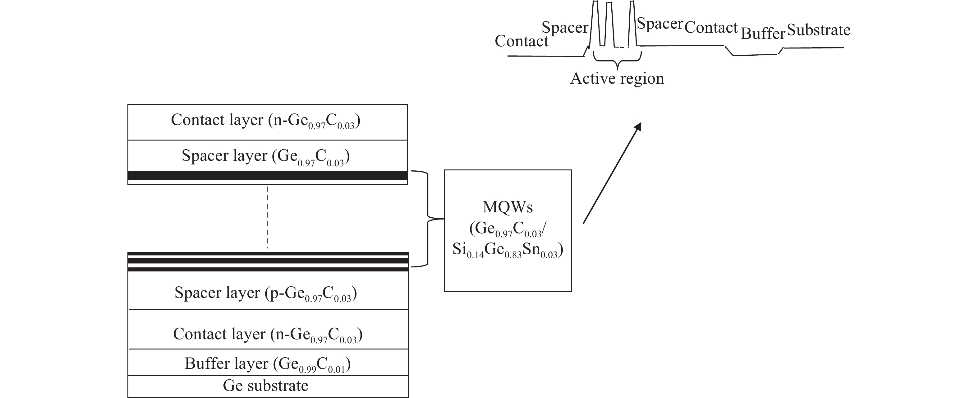
Fig. 1.
Schematic structure of MQW RTD with carriers’ movement.
SEMICONDUCTOR DEVICES
Swagata Dey1, , Vedatrayee Chakraborty2, Bratati Mukhopadhyay1 and Gopa Sen1
Corresponding author: Swagata Dey, swagatadey2009@gmail.com
Abstract: The double barrier quantum well (DBQW) resonant tunneling diode (RTD) structure made of SiGeSn/GeC/SiGeSn alloys grown on Ge substrate is analyzed. The tensile strained Ge1?zCz on Si1?x?yGexSny heterostructure provides a direct band gap type I configuration. The transmission coefficient and tunneling current density have been calculated considering single and multiple quantum wells. A comparative study of tunnelling current of the proposed structure is done with the existing RTD structure based on GeSn/SiGeSn DBH. A higher value of the current density for the proposed structure has been obtained.
Key words: DBQW, MQW, RTD, NDR, tunneling current density
| [1] |
Deen M J, Basu P K. Silicon photonics: fundamentals and Devices. Chichester U K John Wiley, 2012.
|
| [2] |
Pavesi L, Lockwood D J. Silicon photonics. New York: Springer, 2004
|
| [3] |
Bauer M , Taraci J, Tolle J, et al. Ge–Sn semiconductors for band-gap and lattice engineering. Appl Phys Lett, 2002, 81: 2992 doi: 10.1063/1.1515133
|
| [4] |
Lee J W, Reed M A. Molecular beam epitaxial growth of AlGaAs/InGaAs resonant tunneling structures. J Vac Sci Technol B, 1987, 5(3): 771 doi: 10.1116/1.583745
|
| [5] |
Ghosh S, Basu P K. The calculated composition of Ge1?zCz/Ge1?x?zSixSny heterostructure grown on Si for direct gap emission from Ge1?zCz at 1.55 μm. Solid State Commun, 2010, 150: 844 doi: 10.1016/j.ssc.2010.02.017
|
| [6] |
Menendez J, Kouvetakis J. Type-I Ge/GeSiSn strained layer heterostructures with a direct Ge band gap. Appl Phys Lett, 2004, 85: 1175 doi: 10.1063/1.1784032
|
| [7] |
Chakraborty V, Mukhopadhyay B. Group IV heterojunction laser structure based on S–Ge–Sn–C around 1550 nm: determination of gain coefficient. Proceedings in International Conference in Computers andDevices for Communication, 2015
|
| [8] |
Sun G, Soref R A, Cheng H H. Design of an electrically pumped SiGeSn/GeSn/SiGeSn double heterostructure mid infra red laser. J Appl Phys, 2010, 108: 033107 doi: 10.1063/1.3467766
|
| [9] |
Chang S W, Chuang S L. Theory of optical gain of Ge-SixGeySn1?x?y quantum-well lasers. IEEE J Quantum Electron, 2007, 43(3): 249 doi: 10.1109/JQE.2006.890401
|
| [10] |
Zhu Y H, Xu Q, Fan W J, et al. Theoretical gain of strained GeSn/Ge1?x?ySixSny quantum well laser. J Appl Phys, 2010, 107: 073108 doi: 10.1063/1.3329424
|
| [11] |
Chang G E, Chang S W, Chuang S L. Strain-balanced GezSn1?z–SixGeySn1?x?y multiple quantum-well lasers. IEEE J Quantum Electron, 2010, 46(12): 1813 doi: 10.1109/JQE.2010.2059000
|
| [12] |
Basu R, Chakraborty V, Mukhopadhyay B, et al. Predicted performance of Ge/GeSn hetero-photo transistors on Si substrate at 1.55 μm. Opt Quant Electron, 2013, 47(2): 387
|
| [13] |
Moontragoon P, Vukmirovi'C N, Ikoni'C Z, et al. SnGe asymmetric quantum well electro absorption modulators for long-wave silicon photonics. IEEE J Sel Top Quantum Electron, 2010, 16(1): 100 doi: 10.1109/JSTQE.2009.2026691
|
| [14] |
Dey S, Mukhopadhyay B, Basu P K. Modeling of responsivity of GeSn/SiGeSn QWIP. Proceedings in International Conference in Computers andDevices for Communication, 2015
|
| [15] |
Esaki L, Tsu R. Superlattics and negative differential conductivity in semiconductors. IBM J Res Develop, 1970, 14: 61 doi: 10.1147/rd.141.0061
|
| [16] |
Tsu R, Esaki L. Tunneling in a finite superlattice. Appl Phys Lett, 1973, 22: 562 doi: 10.1063/1.1654509
|
| [17] |
Chang L L, Esaki L, Tsu R. Resonant tunnelling in semiconductor double barriers. Appl Phys Lett, 1974, 24: 593 doi: 10.1063/1.1655067
|
| [18] |
Wu K Y, Tsai B H, Chen J Z, et al. Sn-based group-IV structure for resonant tunneling diodes. IEEE Electron Device Lett, 2013, 34(8): 951 doi: 10.1109/LED.2013.2266540
|
| [19] |
Mukherjee K, Das N R. Tunneling current calculations for nonuniform and asymmetric multiple quantum well structures. J Appl Phys, 2011, 109: 053708 doi: 10.1063/1.3553391
|
| [20] |
Handbook of mathematical functions. Edited by Abramowitz M A and Stegun I A. Dover, New York, 1965
|
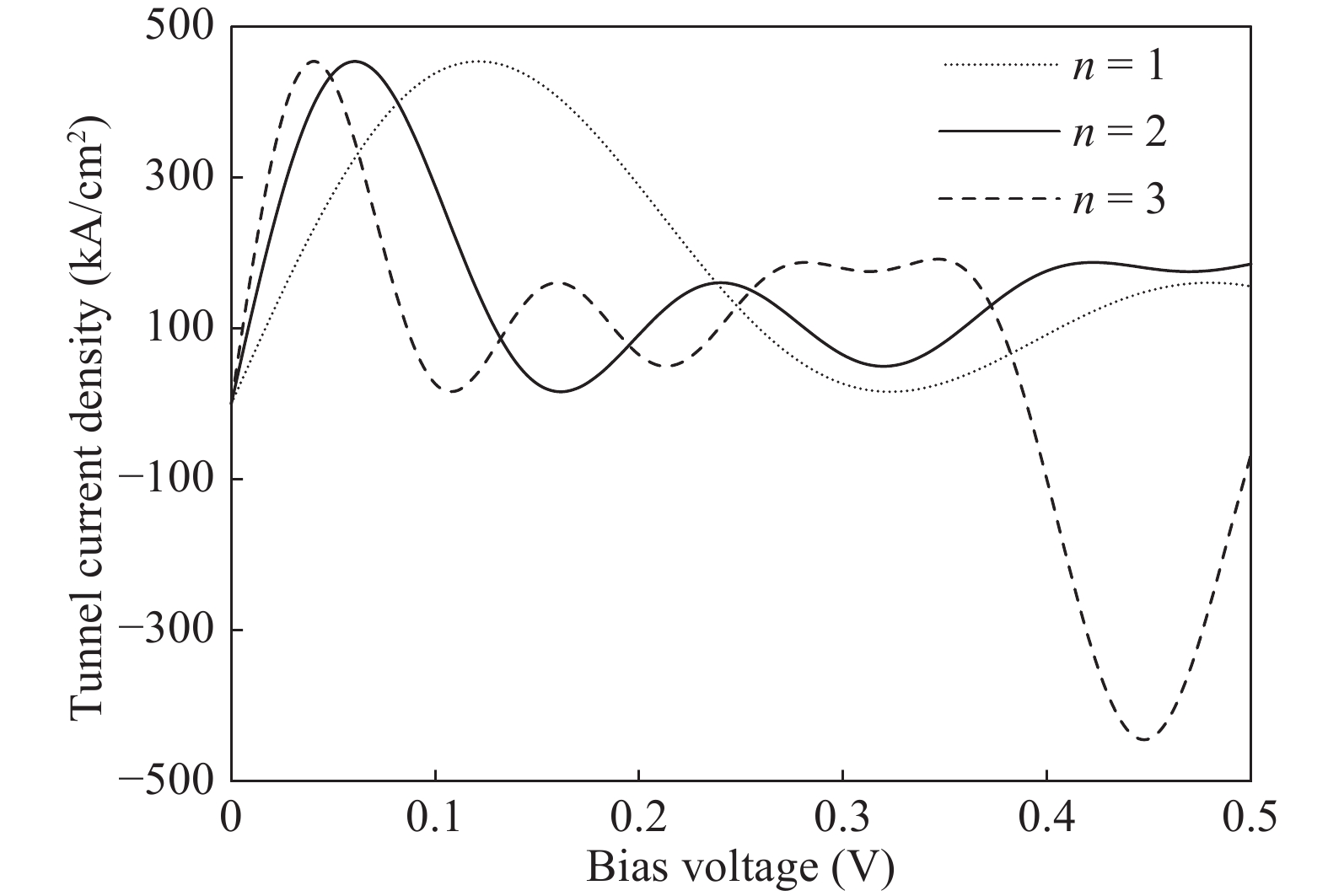
Table 1. Parameters used for calculation.
| Parameter | Si | Ge | C | Sn | ||
| a (?) | 5.4307 | 5.6573 | 3.567 | 6.4892 | ||
| Edir (eV) | 3.3021 | 0.804 | 6.5 | ?0.4102 | ||
| Eind (eV) | 2.1021 | 0.7013 | 9.2 | 0.1202 | ||
| Δ0 (eV) | 0.044 | 0.3 | 0 | 0.8 | ||
| C11 (Pa) | 16.67 | 12.853 | 107.9 | 6.9 | ||
| C12 (Pa) | 6.93 | 4.826 | – | 2.93 | ||
| b = b1 + 2b2 (eV) | ?2.2 | ?2.86 | ?4.67 | – | ||
| av (eV) | 2.46 | 1.24 | ?13.9 | 1.58 | ||
| ac (eV) | ?10.06 | ?8.24 | ?16.8 | ?6.00 | ||


|
1.5 | ?2.34 | – | – |
 DownLoad: CSV
| [1] |
Deen M J, Basu P K. Silicon photonics: fundamentals and Devices. Chichester U K John Wiley, 2012.
|
| [2] |
Pavesi L, Lockwood D J. Silicon photonics. New York: Springer, 2004
|
| [3] |
Bauer M , Taraci J, Tolle J, et al. Ge–Sn semiconductors for band-gap and lattice engineering. Appl Phys Lett, 2002, 81: 2992 doi: 10.1063/1.1515133
|
| [4] |
Lee J W, Reed M A. Molecular beam epitaxial growth of AlGaAs/InGaAs resonant tunneling structures. J Vac Sci Technol B, 1987, 5(3): 771 doi: 10.1116/1.583745
|
| [5] |
Ghosh S, Basu P K. The calculated composition of Ge1?zCz/Ge1?x?zSixSny heterostructure grown on Si for direct gap emission from Ge1?zCz at 1.55 μm. Solid State Commun, 2010, 150: 844 doi: 10.1016/j.ssc.2010.02.017
|
| [6] |
Menendez J, Kouvetakis J. Type-I Ge/GeSiSn strained layer heterostructures with a direct Ge band gap. Appl Phys Lett, 2004, 85: 1175 doi: 10.1063/1.1784032
|
| [7] |
Chakraborty V, Mukhopadhyay B. Group IV heterojunction laser structure based on S–Ge–Sn–C around 1550 nm: determination of gain coefficient. Proceedings in International Conference in Computers andDevices for Communication, 2015
|
| [8] |
Sun G, Soref R A, Cheng H H. Design of an electrically pumped SiGeSn/GeSn/SiGeSn double heterostructure mid infra red laser. J Appl Phys, 2010, 108: 033107 doi: 10.1063/1.3467766
|
| [9] |
Chang S W, Chuang S L. Theory of optical gain of Ge-SixGeySn1?x?y quantum-well lasers. IEEE J Quantum Electron, 2007, 43(3): 249 doi: 10.1109/JQE.2006.890401
|
| [10] |
Zhu Y H, Xu Q, Fan W J, et al. Theoretical gain of strained GeSn/Ge1?x?ySixSny quantum well laser. J Appl Phys, 2010, 107: 073108 doi: 10.1063/1.3329424
|
| [11] |
Chang G E, Chang S W, Chuang S L. Strain-balanced GezSn1?z–SixGeySn1?x?y multiple quantum-well lasers. IEEE J Quantum Electron, 2010, 46(12): 1813 doi: 10.1109/JQE.2010.2059000
|
| [12] |
Basu R, Chakraborty V, Mukhopadhyay B, et al. Predicted performance of Ge/GeSn hetero-photo transistors on Si substrate at 1.55 μm. Opt Quant Electron, 2013, 47(2): 387
|
| [13] |
Moontragoon P, Vukmirovi'C N, Ikoni'C Z, et al. SnGe asymmetric quantum well electro absorption modulators for long-wave silicon photonics. IEEE J Sel Top Quantum Electron, 2010, 16(1): 100 doi: 10.1109/JSTQE.2009.2026691
|
| [14] |
Dey S, Mukhopadhyay B, Basu P K. Modeling of responsivity of GeSn/SiGeSn QWIP. Proceedings in International Conference in Computers andDevices for Communication, 2015
|
| [15] |
Esaki L, Tsu R. Superlattics and negative differential conductivity in semiconductors. IBM J Res Develop, 1970, 14: 61 doi: 10.1147/rd.141.0061
|
| [16] |
Tsu R, Esaki L. Tunneling in a finite superlattice. Appl Phys Lett, 1973, 22: 562 doi: 10.1063/1.1654509
|
| [17] |
Chang L L, Esaki L, Tsu R. Resonant tunnelling in semiconductor double barriers. Appl Phys Lett, 1974, 24: 593 doi: 10.1063/1.1655067
|
| [18] |
Wu K Y, Tsai B H, Chen J Z, et al. Sn-based group-IV structure for resonant tunneling diodes. IEEE Electron Device Lett, 2013, 34(8): 951 doi: 10.1109/LED.2013.2266540
|
| [19] |
Mukherjee K, Das N R. Tunneling current calculations for nonuniform and asymmetric multiple quantum well structures. J Appl Phys, 2011, 109: 053708 doi: 10.1063/1.3553391
|
| [20] |
Handbook of mathematical functions. Edited by Abramowitz M A and Stegun I A. Dover, New York, 1965
|


Article views: 5138 Times PDF downloads: 90 Times Cited by: 0 Times
Received: 06 February 2018 Revised: 07 March 2018 Online: Accepted Manuscript: 23 April 2018Uncorrected proof: 25 April 2018Published: 09 October 2018
| Citation: |
Swagata Dey, Vedatrayee Chakraborty, Bratati Mukhopadhyay, Gopa Sen. Modeling of tunneling current density of GeC based double barrier multiple quantum well resonant tunneling diode[J]. Journal of Semiconductors, 2018, 39(10): 104003. doi: 10.1088/1674-4926/39/10/104003
****
S Dey, V Chakraborty, B Mukhopadhyay, G Sen, Modeling of tunneling current density of GeC based double barrier multiple quantum well resonant tunneling diode[J]. J. Semicond., 2018, 39(10): 104003. doi: 10.1088/1674-4926/39/10/104003.

|
| [1] |
Deen M J, Basu P K. Silicon photonics: fundamentals and Devices. Chichester U K John Wiley, 2012.
|
| [2] |
Pavesi L, Lockwood D J. Silicon photonics. New York: Springer, 2004
|
| [3] |
Bauer M , Taraci J, Tolle J, et al. Ge–Sn semiconductors for band-gap and lattice engineering. Appl Phys Lett, 2002, 81: 2992 doi: 10.1063/1.1515133
|
| [4] |
Lee J W, Reed M A. Molecular beam epitaxial growth of AlGaAs/InGaAs resonant tunneling structures. J Vac Sci Technol B, 1987, 5(3): 771 doi: 10.1116/1.583745
|
| [5] |
Ghosh S, Basu P K. The calculated composition of Ge1?zCz/Ge1?x?zSixSny heterostructure grown on Si for direct gap emission from Ge1?zCz at 1.55 μm. Solid State Commun, 2010, 150: 844 doi: 10.1016/j.ssc.2010.02.017
|
| [6] |
Menendez J, Kouvetakis J. Type-I Ge/GeSiSn strained layer heterostructures with a direct Ge band gap. Appl Phys Lett, 2004, 85: 1175 doi: 10.1063/1.1784032
|
| [7] |
Chakraborty V, Mukhopadhyay B. Group IV heterojunction laser structure based on S–Ge–Sn–C around 1550 nm: determination of gain coefficient. Proceedings in International Conference in Computers andDevices for Communication, 2015
|
| [8] |
Sun G, Soref R A, Cheng H H. Design of an electrically pumped SiGeSn/GeSn/SiGeSn double heterostructure mid infra red laser. J Appl Phys, 2010, 108: 033107 doi: 10.1063/1.3467766
|
| [9] |
Chang S W, Chuang S L. Theory of optical gain of Ge-SixGeySn1?x?y quantum-well lasers. IEEE J Quantum Electron, 2007, 43(3): 249 doi: 10.1109/JQE.2006.890401
|
| [10] |
Zhu Y H, Xu Q, Fan W J, et al. Theoretical gain of strained GeSn/Ge1?x?ySixSny quantum well laser. J Appl Phys, 2010, 107: 073108 doi: 10.1063/1.3329424
|
| [11] |
Chang G E, Chang S W, Chuang S L. Strain-balanced GezSn1?z–SixGeySn1?x?y multiple quantum-well lasers. IEEE J Quantum Electron, 2010, 46(12): 1813 doi: 10.1109/JQE.2010.2059000
|
| [12] |
Basu R, Chakraborty V, Mukhopadhyay B, et al. Predicted performance of Ge/GeSn hetero-photo transistors on Si substrate at 1.55 μm. Opt Quant Electron, 2013, 47(2): 387
|
| [13] |
Moontragoon P, Vukmirovi'C N, Ikoni'C Z, et al. SnGe asymmetric quantum well electro absorption modulators for long-wave silicon photonics. IEEE J Sel Top Quantum Electron, 2010, 16(1): 100 doi: 10.1109/JSTQE.2009.2026691
|
| [14] |
Dey S, Mukhopadhyay B, Basu P K. Modeling of responsivity of GeSn/SiGeSn QWIP. Proceedings in International Conference in Computers andDevices for Communication, 2015
|
| [15] |
Esaki L, Tsu R. Superlattics and negative differential conductivity in semiconductors. IBM J Res Develop, 1970, 14: 61 doi: 10.1147/rd.141.0061
|
| [16] |
Tsu R, Esaki L. Tunneling in a finite superlattice. Appl Phys Lett, 1973, 22: 562 doi: 10.1063/1.1654509
|
| [17] |
Chang L L, Esaki L, Tsu R. Resonant tunnelling in semiconductor double barriers. Appl Phys Lett, 1974, 24: 593 doi: 10.1063/1.1655067
|
| [18] |
Wu K Y, Tsai B H, Chen J Z, et al. Sn-based group-IV structure for resonant tunneling diodes. IEEE Electron Device Lett, 2013, 34(8): 951 doi: 10.1109/LED.2013.2266540
|
| [19] |
Mukherjee K, Das N R. Tunneling current calculations for nonuniform and asymmetric multiple quantum well structures. J Appl Phys, 2011, 109: 053708 doi: 10.1063/1.3553391
|
| [20] |
Handbook of mathematical functions. Edited by Abramowitz M A and Stegun I A. Dover, New York, 1965
|

 WeChat ID
Journal of Semiconductors © 2017 All Rights Reserved 京ICP備05085259號-2

