


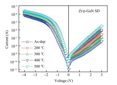
Fig. 1.
(Color online) Reverse and forward current-voltage (I-V) characteristics of the Zr/p-GaN Schottky diode at different annealing temperatures.
SEMICONDUCTOR DEVICES
V. Rajagopal Reddy1, , B. Asha1 and Chel-Jong Choi2,
Corresponding author: V. Rajagopal Reddy Email:vrg@rediffmail.com; Chel-Jong Choi Email:cjchoi@chonbuk.ac.kr
Abstract: The Schottky barrier junction parameters and structural properties of Zr/p-GaN Schottky diode are explored at various annealing temperatures. Experimental analysis showed that the barrier height (BH) of the Zr/pGaN Schottky diode increases with annealing at 400℃ (0.92 eV (I-V)/1.09 eV (C-V)compared to the asdeposited one (0.83 eV (I-V)/0.93 eV (C-V). However, the BH decreases after annealing at 500℃. Also, at different annealing temperatures, the series resistance and BH are assessed by Cheung's functions and their values compared. Further, the interface state density (NSS)of the diode decreases after annealing at 400℃ and then somewhat rises upon annealing at 500℃. Analysis reveals that the maximum BH is obtained at 400℃, and thus the optimum annealing temperature is 400℃ for the diode. The XPS and XRD analysis revealed that the increase in BH may be attributed to the creation of Zr-N phases with increasing annealing up to 400℃. The BH reduces for the diode annealed at 500℃, which may be due to the formation of Ga-Zr phases at the junction. The AFM measurements reveal that the overall surface roughness of the Zr film is quite smooth during rapid annealing process.
Key words: zirconium Schottky contacts, p-type GaN, electrical characteristics, energy distribution curves, X-ray photoelectron spectroscopy, X-ray diffraction
| [1] |
Chen L C, Hsu C Y, Lan W H, et al. GaN-based light-emitting diodes with Ni/AuBe transparent conductive layer. Solid State Electron, 2003, 47:1843 doi: 10.1016/S0038-1101(03)00129-1
|
| [2] |
Huang L H, Yeh S H, Lee C T, et al. AlGaN/GaN metal-oxidesemiconductor high-electron mobility transistors using oxide insulator grown by photoelectrochemical oxidation method. IEEE Electron Devices Lett, 2008, 29:284 doi: 10.1109/LED.2008.917326
|
| [3] |
Miyajima T, Watanabe H, Ikeda M, et al. Picosecond optical pulse generation from self-pulsating bisectional GaN-based blue-violet laser diodes. Appl Phys Lett, 2009, 94:161103 doi: 10.1063/1.3106055
|
| [4] |
Ravinandan M, Koteswara Rao P, Rajagopal Reddy V. Analysis of the current-voltage characteristics of the Pd/Au Schottky structure on n-type GaN in a wide temperature range. Semicond Sci Technol, 2009, 24:035004 doi: 10.1088/0268-1242/24/3/035004
|
| [5] |
Kim T K, Kim S H, Yang S S, et al. GaN-based light-emitting diode with textured indium tin oxide transparent layer coated with Al2O3 powder. Appl Phys Lett, 2009, 94:161107 doi: 10.1063/1.3120222
|
| [6] |
Takahashi K, Ao J P, Ikawa Y, et al. GaN Schottky diodes for microwave power rectification. Jpn J Appl Phys, 2009, 48:04C095 doi: 10.1143/JJAP.48.04C095/pdf
|
| [7] |
Hu W D, Chen X S, Yin F, et al. Two-dimensional transient simulations of drain lag and current collapse in GaN-based high-electron-mobility transistors. J Appl Phys, 2009, 105:084502 doi: 10.1063/1.3106603
|
| [8] |
Korona K P, Drabinska A, Caban P, et al. Tunable GaN/AlGaN ultraviolet detectors with built-in electric field. J Appl Phys, 2009, 105:083712 doi: 10.1063/1.3110106
|
| [9] |
Chen Z, Pei Y, Newman S, et al. Growth of AlGaN/GaN heterojunction field effect transistors on semi-insulating GaN using an AlGaN interlayer. Appl Phys Lett, 2009, 94:112108 doi: 10.1063/1.3103210
|
| [10] |
Lin J C, Su Y K, Chang S J, et al. High responsivity of GaN p-i-np-i-n photodiode by using low-temperature interlayer. Appl Phys Lett, 2007, 91:173502 doi: 10.1063/1.2800813
|
| [11] |
Wu J. When group-Ⅲ nitrides go infrared:new properties and perspectives. J Appl Phys, 2009, 106:011101 doi: 10.1063/1.3155798
|
| [12] |
Yu L S, Qiao D, Jia L, et al. Study of Schottky barrier of Ni on p-GaN. Appl Phys Lett, 2001, 97:4536 doi: 10.1063/1.1428773
|
| [13] |
Kim J W, Lee J W. Ti/Al p-GaN Schottky barrier height determined by C -V measurements. Appl Surf Sci, 2005, 250:247 doi: 10.1016/j.apsusc.2005.01.004
|
| [14] |
Tan C K, Abdul Aziz A, Yam F K. Schottky barrier properties of various metal (Zr, Ti, Cr, Pt) contact on p-GaN revealed from I -V -T measurement. Appl Surf Sci, 2006, 252:5930 doi: 10.1016/j.apsusc.2005.08.018
|
| [15] |
Fukushima Y, Ogisu K, Kuzuhara M, et al. I -V and C -V characteristics of rare-earth-metal/p-GaN Schottky contacts. Phys Status Solidi C, 2009, 6:S856 doi: 10.1002/pssc.v6.5s2
|
| [16] |
Jang S H, Jang J S. Electrical characteristics and carrier transport mechanism for Ti/p-GaN Schottky diodes. Electron Mater Lett, 2013, 9:245 doi: 10.1007/s13391-012-2175-y
|
| [17] |
Nagaraju G, Dasaradha Rao L, Rajagopal Reddy V. Annealing effects on the electrical, structural and morphological properties of Ti/p-GaN/Ni/Au Schottky diode. Appl Phys A, 2015, 121:131 https://www.researchgate.net/profile/Dasaradha_Lambada/publication/280624228_Annealing_effects_on_the_electrical_structural_and_morphological_properties_of_Tip-GaNNiAu_Schottky_diode/links/55bf844f08aed621de139800.pdf
|
| [18] |
Padma R, Nagaraju G, Rajagopal R V, et al. Effect of annealing temperature on the electrical and structural properties of V/pGaN Schottky structures. Thin Solid Films, 2016, 598:236 doi: 10.1016/j.tsf.2015.12.018
|
| [19] |
Aoki T, Tanikawa T, Katayama R, et al. Electrical characteristics of N-polar (000T) p-type GaN Schottky contacts. Jpn J Appl Phys, 2016, 55:04EJ09 doi: 10.7567/JJAP.55.04EJ09/pdf
|
| [20] |
Rajagopal Reddy V, Asha B, Choi C J. Effects of annealing on electrical characteristics and current transport mechanisms of the Y/p-GaN Schottky diode. J Electron Mater, 2016, 45:3268 doi: 10.1007/s11664-016-4490-9
|
| [21] |
Rhoderick E H, Williams R H. Metal-semiconductor contacts. Oxford:Clarendon, 1988
|
| [22] |
Altindal S, Karadeniz S, Tugluoglu N, et al. The role of interface states and series resistance on the I -V and C -V characteristics in Al/SnO2/p-Si Schottky diodes. Solid State Electron, 2003, 47:1847 doi: 10.1016/S0038-1101(03)00182-5
|
| [23] |
Tung R T. Electron transport at metal-semiconductor interfaces:general theory. Phys Rev B, 1992, 45:13509 doi: 10.1103/PhysRevB.45.13509
|
| [24] |
Sze S M. Physics of semiconductor devices. 2nd ed. New York:Willey, 1981
|
| [25] |
Cheung S K, Cheung N W. Extraction of Schottky diode parameters from forward current-voltage characteristics. Appl Phys Lett, 1986, 49:85 doi: 10.1063/1.97359
|
| [26] |
Mohan G D. Fluctuations in Schottky barrier heights. J Appl Phys, 1984, 55:980 doi: 10.1063/1.333153
|
| [27] |
Song Y P, Van Meirhaeghe R L, Laflere W H, et al. On the difference in apparent barrier height as obtained from capacitancevoltage and current-voltage-temperature measurements on Al/pInP Schottky barriers. Solid State Electron, 1986, 29:633 doi: 10.1016/0038-1101(86)90145-0
|
| [28] |
Werner J H, Guttler H H. Barrier inhomogeneities at Schottky contacts. J Appl Phys, 1991, 69:1522 doi: 10.1063/1.347243
|
| [29] |
Boyarbay B, Cetin H, Kaya M, et al. Correlation between barrier heights and ideality factors of H-terminated Sn/p-Si(100) Schottky barrier diodes. Microelectron Eng, 2008, 85:721 doi: 10.1016/j.mee.2008.01.005
|
| [30] |
Geng L, Ponce F A, Tanaka S, et al. Surface morphology of AlxGa1-xN films grown by MOCVD. Phys Stat Sol A, 2001, 188:803 doi: 10.1002/(ISSN)1521-396X
|
| [31] |
Card H C, Rhoderick E H. Studies of tunnel MOS diodes Ⅱ. thermal equilibrium considerations. J Phys D Appl Phys, 1971, 4:1589 doi: 10.1088/0022-3727/4/10/319
|
| [32] |
Rajagopal Reddy V. Electrical properties and conduction mechanism of an organic-modified Au/NiPc/n-InP Schottky barrier diode. Appl Phys A, 2014, 116:1379 doi: 10.1007/s00339-014-8238-1
|
| [33] |
Karatas S, Altindal S, Turut A, et al. Temperature dependence of characteristic parameters of the H-terminated Sn/p-Si(100) Schottky contacts. Appl Surf Sci, 2003, 217:250 doi: 10.1016/S0169-4332(03)00564-6
|
| [34] |
Karatas S, Turut A. The determination of electronic and interface state density distributions of Au/n-type GaAs Schottky barrier diodes. Physica B, 2006, 381:199 doi: 10.1016/j.physb.2006.01.412
|
| [35] |
Prasanna Lakshmi B, Rajagopal Reddy V, Janardhanam V, et al. Effect of annealing temperature on the electrical properties of Au/Ta2O5/n-GaN metal-insulator-semiconductor (MIS) structure. Appl Phys A, 2013, 113:713 doi: 10.1007/s00339-013-7797-x
|
| [36] |
Monch W. Semiconductor surfaces and interfaces. 3rd ed. Berlin:Springer, 2001
|
| [37] |
Huang T S, Fang R S. Barrier height enhancement of Pt/n-InP Schottky diodes by P2S5/(NH4)2S solution treatment of the InP surface. Solid State Electron, 1994, 37:1461 doi: 10.1016/0038-1101(94)90152-X
|
| [38] |
Guo J D, Pan F M, Feng M S, et al. Schottky contact and the thermal stability of Ni on n-type GaN. J Appl Phys, 1996, 80:1623 doi: 10.1063/1.363822
|
| [39] |
Rajagopal Reddy V, Koteswara Rao P. Annealing temperature effect on electrical and structural properties of Cu/Au Schottky contacts to n-type GaN. Microelectron Eng, 2008, 85:470 doi: 10.1016/j.mee.2007.08.006
|
| [40] |
Siva Pratap Reddy M, Rajagopal Reddy V, Choi C J. Electrical properties and interfacial reactions of rapidly annealed Ni/Ru Schottky rectifiers on n-type GaN. J Alloys Compd, 2010, 503:186 doi: 10.1016/j.jallcom.2010.04.230
|
| [41] |
Jyothi I, Rajagopal Reddy V, Choi C J. Microstructural and electrical characteristics of rapidly annealed Ni/Mo Schottky rectifiers on cleaned n-type GaN (0001) surface. J Mater Sci Mater Electron, 2011, 22:286 doi: 10.1007/s10854-010-0129-4
|
| [42] |
Nanda Kumar Reddy N, Rajagopal Reddy V, Choi C J. Influence of rapid thermal annealing effect on electrical and structural properties of Pd/Ru Schottky contacts to n-type GaN. Mater Chem Phys, 2011, 130:1000 doi: 10.1016/j.matchemphys.2011.08.026
|
| [43] |
Wang J, Zhao D G, Sun Y P, et al. Thermal annealing behaviour of Pt on n-GaN Schottky contacts. J Phys D Appl Phys, 2003, 36:1018 doi: 10.1088/0022-3727/36/8/312
|
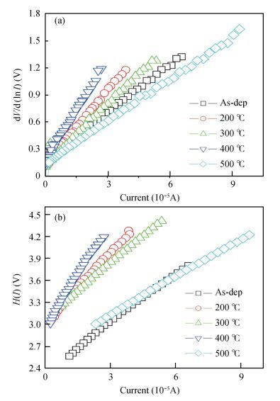
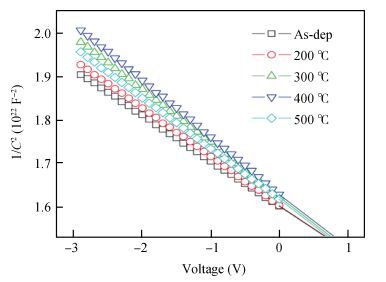
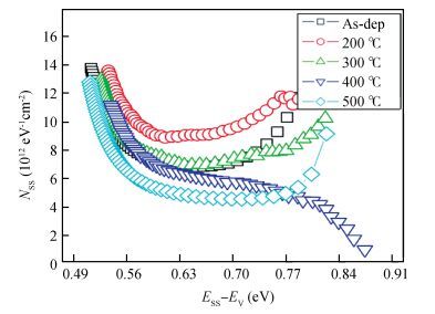
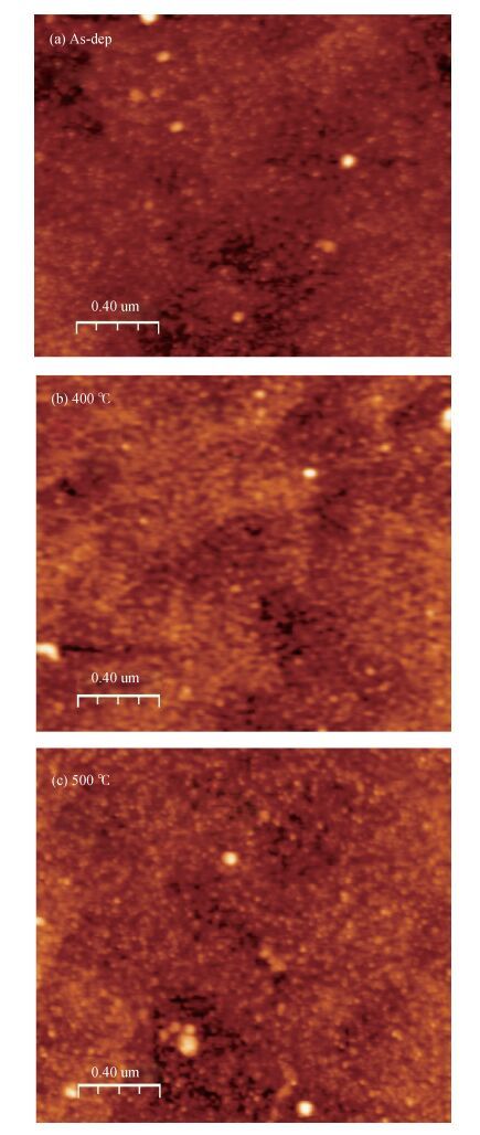
Table 1. Review on different Schottky contacts on p-GaN.
 |
Table 2. The calculated barrier height, ideality factor, series resistance and interface state density of the Zr/p-GaN Schottky diode by I-V and C-V techniques at different annealing temperatures.
 |
| [1] |
Chen L C, Hsu C Y, Lan W H, et al. GaN-based light-emitting diodes with Ni/AuBe transparent conductive layer. Solid State Electron, 2003, 47:1843 doi: 10.1016/S0038-1101(03)00129-1
|
| [2] |
Huang L H, Yeh S H, Lee C T, et al. AlGaN/GaN metal-oxidesemiconductor high-electron mobility transistors using oxide insulator grown by photoelectrochemical oxidation method. IEEE Electron Devices Lett, 2008, 29:284 doi: 10.1109/LED.2008.917326
|
| [3] |
Miyajima T, Watanabe H, Ikeda M, et al. Picosecond optical pulse generation from self-pulsating bisectional GaN-based blue-violet laser diodes. Appl Phys Lett, 2009, 94:161103 doi: 10.1063/1.3106055
|
| [4] |
Ravinandan M, Koteswara Rao P, Rajagopal Reddy V. Analysis of the current-voltage characteristics of the Pd/Au Schottky structure on n-type GaN in a wide temperature range. Semicond Sci Technol, 2009, 24:035004 doi: 10.1088/0268-1242/24/3/035004
|
| [5] |
Kim T K, Kim S H, Yang S S, et al. GaN-based light-emitting diode with textured indium tin oxide transparent layer coated with Al2O3 powder. Appl Phys Lett, 2009, 94:161107 doi: 10.1063/1.3120222
|
| [6] |
Takahashi K, Ao J P, Ikawa Y, et al. GaN Schottky diodes for microwave power rectification. Jpn J Appl Phys, 2009, 48:04C095 doi: 10.1143/JJAP.48.04C095/pdf
|
| [7] |
Hu W D, Chen X S, Yin F, et al. Two-dimensional transient simulations of drain lag and current collapse in GaN-based high-electron-mobility transistors. J Appl Phys, 2009, 105:084502 doi: 10.1063/1.3106603
|
| [8] |
Korona K P, Drabinska A, Caban P, et al. Tunable GaN/AlGaN ultraviolet detectors with built-in electric field. J Appl Phys, 2009, 105:083712 doi: 10.1063/1.3110106
|
| [9] |
Chen Z, Pei Y, Newman S, et al. Growth of AlGaN/GaN heterojunction field effect transistors on semi-insulating GaN using an AlGaN interlayer. Appl Phys Lett, 2009, 94:112108 doi: 10.1063/1.3103210
|
| [10] |
Lin J C, Su Y K, Chang S J, et al. High responsivity of GaN p-i-np-i-n photodiode by using low-temperature interlayer. Appl Phys Lett, 2007, 91:173502 doi: 10.1063/1.2800813
|
| [11] |
Wu J. When group-Ⅲ nitrides go infrared:new properties and perspectives. J Appl Phys, 2009, 106:011101 doi: 10.1063/1.3155798
|
| [12] |
Yu L S, Qiao D, Jia L, et al. Study of Schottky barrier of Ni on p-GaN. Appl Phys Lett, 2001, 97:4536 doi: 10.1063/1.1428773
|
| [13] |
Kim J W, Lee J W. Ti/Al p-GaN Schottky barrier height determined by C -V measurements. Appl Surf Sci, 2005, 250:247 doi: 10.1016/j.apsusc.2005.01.004
|
| [14] |
Tan C K, Abdul Aziz A, Yam F K. Schottky barrier properties of various metal (Zr, Ti, Cr, Pt) contact on p-GaN revealed from I -V -T measurement. Appl Surf Sci, 2006, 252:5930 doi: 10.1016/j.apsusc.2005.08.018
|
| [15] |
Fukushima Y, Ogisu K, Kuzuhara M, et al. I -V and C -V characteristics of rare-earth-metal/p-GaN Schottky contacts. Phys Status Solidi C, 2009, 6:S856 doi: 10.1002/pssc.v6.5s2
|
| [16] |
Jang S H, Jang J S. Electrical characteristics and carrier transport mechanism for Ti/p-GaN Schottky diodes. Electron Mater Lett, 2013, 9:245 doi: 10.1007/s13391-012-2175-y
|
| [17] |
Nagaraju G, Dasaradha Rao L, Rajagopal Reddy V. Annealing effects on the electrical, structural and morphological properties of Ti/p-GaN/Ni/Au Schottky diode. Appl Phys A, 2015, 121:131 https://www.researchgate.net/profile/Dasaradha_Lambada/publication/280624228_Annealing_effects_on_the_electrical_structural_and_morphological_properties_of_Tip-GaNNiAu_Schottky_diode/links/55bf844f08aed621de139800.pdf
|
| [18] |
Padma R, Nagaraju G, Rajagopal R V, et al. Effect of annealing temperature on the electrical and structural properties of V/pGaN Schottky structures. Thin Solid Films, 2016, 598:236 doi: 10.1016/j.tsf.2015.12.018
|
| [19] |
Aoki T, Tanikawa T, Katayama R, et al. Electrical characteristics of N-polar (000T) p-type GaN Schottky contacts. Jpn J Appl Phys, 2016, 55:04EJ09 doi: 10.7567/JJAP.55.04EJ09/pdf
|
| [20] |
Rajagopal Reddy V, Asha B, Choi C J. Effects of annealing on electrical characteristics and current transport mechanisms of the Y/p-GaN Schottky diode. J Electron Mater, 2016, 45:3268 doi: 10.1007/s11664-016-4490-9
|
| [21] |
Rhoderick E H, Williams R H. Metal-semiconductor contacts. Oxford:Clarendon, 1988
|
| [22] |
Altindal S, Karadeniz S, Tugluoglu N, et al. The role of interface states and series resistance on the I -V and C -V characteristics in Al/SnO2/p-Si Schottky diodes. Solid State Electron, 2003, 47:1847 doi: 10.1016/S0038-1101(03)00182-5
|
| [23] |
Tung R T. Electron transport at metal-semiconductor interfaces:general theory. Phys Rev B, 1992, 45:13509 doi: 10.1103/PhysRevB.45.13509
|
| [24] |
Sze S M. Physics of semiconductor devices. 2nd ed. New York:Willey, 1981
|
| [25] |
Cheung S K, Cheung N W. Extraction of Schottky diode parameters from forward current-voltage characteristics. Appl Phys Lett, 1986, 49:85 doi: 10.1063/1.97359
|
| [26] |
Mohan G D. Fluctuations in Schottky barrier heights. J Appl Phys, 1984, 55:980 doi: 10.1063/1.333153
|
| [27] |
Song Y P, Van Meirhaeghe R L, Laflere W H, et al. On the difference in apparent barrier height as obtained from capacitancevoltage and current-voltage-temperature measurements on Al/pInP Schottky barriers. Solid State Electron, 1986, 29:633 doi: 10.1016/0038-1101(86)90145-0
|
| [28] |
Werner J H, Guttler H H. Barrier inhomogeneities at Schottky contacts. J Appl Phys, 1991, 69:1522 doi: 10.1063/1.347243
|
| [29] |
Boyarbay B, Cetin H, Kaya M, et al. Correlation between barrier heights and ideality factors of H-terminated Sn/p-Si(100) Schottky barrier diodes. Microelectron Eng, 2008, 85:721 doi: 10.1016/j.mee.2008.01.005
|
| [30] |
Geng L, Ponce F A, Tanaka S, et al. Surface morphology of AlxGa1-xN films grown by MOCVD. Phys Stat Sol A, 2001, 188:803 doi: 10.1002/(ISSN)1521-396X
|
| [31] |
Card H C, Rhoderick E H. Studies of tunnel MOS diodes Ⅱ. thermal equilibrium considerations. J Phys D Appl Phys, 1971, 4:1589 doi: 10.1088/0022-3727/4/10/319
|
| [32] |
Rajagopal Reddy V. Electrical properties and conduction mechanism of an organic-modified Au/NiPc/n-InP Schottky barrier diode. Appl Phys A, 2014, 116:1379 doi: 10.1007/s00339-014-8238-1
|
| [33] |
Karatas S, Altindal S, Turut A, et al. Temperature dependence of characteristic parameters of the H-terminated Sn/p-Si(100) Schottky contacts. Appl Surf Sci, 2003, 217:250 doi: 10.1016/S0169-4332(03)00564-6
|
| [34] |
Karatas S, Turut A. The determination of electronic and interface state density distributions of Au/n-type GaAs Schottky barrier diodes. Physica B, 2006, 381:199 doi: 10.1016/j.physb.2006.01.412
|
| [35] |
Prasanna Lakshmi B, Rajagopal Reddy V, Janardhanam V, et al. Effect of annealing temperature on the electrical properties of Au/Ta2O5/n-GaN metal-insulator-semiconductor (MIS) structure. Appl Phys A, 2013, 113:713 doi: 10.1007/s00339-013-7797-x
|
| [36] |
Monch W. Semiconductor surfaces and interfaces. 3rd ed. Berlin:Springer, 2001
|
| [37] |
Huang T S, Fang R S. Barrier height enhancement of Pt/n-InP Schottky diodes by P2S5/(NH4)2S solution treatment of the InP surface. Solid State Electron, 1994, 37:1461 doi: 10.1016/0038-1101(94)90152-X
|
| [38] |
Guo J D, Pan F M, Feng M S, et al. Schottky contact and the thermal stability of Ni on n-type GaN. J Appl Phys, 1996, 80:1623 doi: 10.1063/1.363822
|
| [39] |
Rajagopal Reddy V, Koteswara Rao P. Annealing temperature effect on electrical and structural properties of Cu/Au Schottky contacts to n-type GaN. Microelectron Eng, 2008, 85:470 doi: 10.1016/j.mee.2007.08.006
|
| [40] |
Siva Pratap Reddy M, Rajagopal Reddy V, Choi C J. Electrical properties and interfacial reactions of rapidly annealed Ni/Ru Schottky rectifiers on n-type GaN. J Alloys Compd, 2010, 503:186 doi: 10.1016/j.jallcom.2010.04.230
|
| [41] |
Jyothi I, Rajagopal Reddy V, Choi C J. Microstructural and electrical characteristics of rapidly annealed Ni/Mo Schottky rectifiers on cleaned n-type GaN (0001) surface. J Mater Sci Mater Electron, 2011, 22:286 doi: 10.1007/s10854-010-0129-4
|
| [42] |
Nanda Kumar Reddy N, Rajagopal Reddy V, Choi C J. Influence of rapid thermal annealing effect on electrical and structural properties of Pd/Ru Schottky contacts to n-type GaN. Mater Chem Phys, 2011, 130:1000 doi: 10.1016/j.matchemphys.2011.08.026
|
| [43] |
Wang J, Zhao D G, Sun Y P, et al. Thermal annealing behaviour of Pt on n-GaN Schottky contacts. J Phys D Appl Phys, 2003, 36:1018 doi: 10.1088/0022-3727/36/8/312
|


Article views: 5616 Times PDF downloads: 120 Times Cited by: 0 Times
Received: 06 November 2016 Revised: 06 December 2016 Online: Published: 01 June 2017
| Citation: |
V. Rajagopal Reddy, B. Asha, Chel-Jong Choi. Schottky barrier parameters and structural properties of rapidly annealed Zr Schottky electrode on p-type GaN[J]. Journal of Semiconductors, 2017, 38(6): 064001. doi: 10.1088/1674-4926/38/6/064001
****
V R Reddy, B Asha, C J Choi. Schottky barrier parameters and structural properties of rapidly annealed Zr Schottky electrode on p-type GaN[J]. J. Semicond., 2017, 38(6): 064001. doi:? 10.1088/1674-4926/38/6/064001.

|
Funded by the Ministry of Trade, Industry and Energy (MOTIE), Republic of Korea
Project supported by the R & D Program for Industrial Core Technology (No. 10045216) and the Transfer Machine Specialized Lighting Core Technology Development Professional Manpower Training Project (No. N0001363) Funded by the Ministry of Trade, Industry and Energy (MOTIE), Republic of Korea
the Transfer Machine Specialized Lighting Core Technology Development Professional Manpower Training Project No. N0001363
by the R & D Program for Industrial Core Technology No. 10045216
| [1] |
Chen L C, Hsu C Y, Lan W H, et al. GaN-based light-emitting diodes with Ni/AuBe transparent conductive layer. Solid State Electron, 2003, 47:1843 doi: 10.1016/S0038-1101(03)00129-1
|
| [2] |
Huang L H, Yeh S H, Lee C T, et al. AlGaN/GaN metal-oxidesemiconductor high-electron mobility transistors using oxide insulator grown by photoelectrochemical oxidation method. IEEE Electron Devices Lett, 2008, 29:284 doi: 10.1109/LED.2008.917326
|
| [3] |
Miyajima T, Watanabe H, Ikeda M, et al. Picosecond optical pulse generation from self-pulsating bisectional GaN-based blue-violet laser diodes. Appl Phys Lett, 2009, 94:161103 doi: 10.1063/1.3106055
|
| [4] |
Ravinandan M, Koteswara Rao P, Rajagopal Reddy V. Analysis of the current-voltage characteristics of the Pd/Au Schottky structure on n-type GaN in a wide temperature range. Semicond Sci Technol, 2009, 24:035004 doi: 10.1088/0268-1242/24/3/035004
|
| [5] |
Kim T K, Kim S H, Yang S S, et al. GaN-based light-emitting diode with textured indium tin oxide transparent layer coated with Al2O3 powder. Appl Phys Lett, 2009, 94:161107 doi: 10.1063/1.3120222
|
| [6] |
Takahashi K, Ao J P, Ikawa Y, et al. GaN Schottky diodes for microwave power rectification. Jpn J Appl Phys, 2009, 48:04C095 doi: 10.1143/JJAP.48.04C095/pdf
|
| [7] |
Hu W D, Chen X S, Yin F, et al. Two-dimensional transient simulations of drain lag and current collapse in GaN-based high-electron-mobility transistors. J Appl Phys, 2009, 105:084502 doi: 10.1063/1.3106603
|
| [8] |
Korona K P, Drabinska A, Caban P, et al. Tunable GaN/AlGaN ultraviolet detectors with built-in electric field. J Appl Phys, 2009, 105:083712 doi: 10.1063/1.3110106
|
| [9] |
Chen Z, Pei Y, Newman S, et al. Growth of AlGaN/GaN heterojunction field effect transistors on semi-insulating GaN using an AlGaN interlayer. Appl Phys Lett, 2009, 94:112108 doi: 10.1063/1.3103210
|
| [10] |
Lin J C, Su Y K, Chang S J, et al. High responsivity of GaN p-i-np-i-n photodiode by using low-temperature interlayer. Appl Phys Lett, 2007, 91:173502 doi: 10.1063/1.2800813
|
| [11] |
Wu J. When group-Ⅲ nitrides go infrared:new properties and perspectives. J Appl Phys, 2009, 106:011101 doi: 10.1063/1.3155798
|
| [12] |
Yu L S, Qiao D, Jia L, et al. Study of Schottky barrier of Ni on p-GaN. Appl Phys Lett, 2001, 97:4536 doi: 10.1063/1.1428773
|
| [13] |
Kim J W, Lee J W. Ti/Al p-GaN Schottky barrier height determined by C -V measurements. Appl Surf Sci, 2005, 250:247 doi: 10.1016/j.apsusc.2005.01.004
|
| [14] |
Tan C K, Abdul Aziz A, Yam F K. Schottky barrier properties of various metal (Zr, Ti, Cr, Pt) contact on p-GaN revealed from I -V -T measurement. Appl Surf Sci, 2006, 252:5930 doi: 10.1016/j.apsusc.2005.08.018
|
| [15] |
Fukushima Y, Ogisu K, Kuzuhara M, et al. I -V and C -V characteristics of rare-earth-metal/p-GaN Schottky contacts. Phys Status Solidi C, 2009, 6:S856 doi: 10.1002/pssc.v6.5s2
|
| [16] |
Jang S H, Jang J S. Electrical characteristics and carrier transport mechanism for Ti/p-GaN Schottky diodes. Electron Mater Lett, 2013, 9:245 doi: 10.1007/s13391-012-2175-y
|
| [17] |
Nagaraju G, Dasaradha Rao L, Rajagopal Reddy V. Annealing effects on the electrical, structural and morphological properties of Ti/p-GaN/Ni/Au Schottky diode. Appl Phys A, 2015, 121:131 https://www.researchgate.net/profile/Dasaradha_Lambada/publication/280624228_Annealing_effects_on_the_electrical_structural_and_morphological_properties_of_Tip-GaNNiAu_Schottky_diode/links/55bf844f08aed621de139800.pdf
|
| [18] |
Padma R, Nagaraju G, Rajagopal R V, et al. Effect of annealing temperature on the electrical and structural properties of V/pGaN Schottky structures. Thin Solid Films, 2016, 598:236 doi: 10.1016/j.tsf.2015.12.018
|
| [19] |
Aoki T, Tanikawa T, Katayama R, et al. Electrical characteristics of N-polar (000T) p-type GaN Schottky contacts. Jpn J Appl Phys, 2016, 55:04EJ09 doi: 10.7567/JJAP.55.04EJ09/pdf
|
| [20] |
Rajagopal Reddy V, Asha B, Choi C J. Effects of annealing on electrical characteristics and current transport mechanisms of the Y/p-GaN Schottky diode. J Electron Mater, 2016, 45:3268 doi: 10.1007/s11664-016-4490-9
|
| [21] |
Rhoderick E H, Williams R H. Metal-semiconductor contacts. Oxford:Clarendon, 1988
|
| [22] |
Altindal S, Karadeniz S, Tugluoglu N, et al. The role of interface states and series resistance on the I -V and C -V characteristics in Al/SnO2/p-Si Schottky diodes. Solid State Electron, 2003, 47:1847 doi: 10.1016/S0038-1101(03)00182-5
|
| [23] |
Tung R T. Electron transport at metal-semiconductor interfaces:general theory. Phys Rev B, 1992, 45:13509 doi: 10.1103/PhysRevB.45.13509
|
| [24] |
Sze S M. Physics of semiconductor devices. 2nd ed. New York:Willey, 1981
|
| [25] |
Cheung S K, Cheung N W. Extraction of Schottky diode parameters from forward current-voltage characteristics. Appl Phys Lett, 1986, 49:85 doi: 10.1063/1.97359
|
| [26] |
Mohan G D. Fluctuations in Schottky barrier heights. J Appl Phys, 1984, 55:980 doi: 10.1063/1.333153
|
| [27] |
Song Y P, Van Meirhaeghe R L, Laflere W H, et al. On the difference in apparent barrier height as obtained from capacitancevoltage and current-voltage-temperature measurements on Al/pInP Schottky barriers. Solid State Electron, 1986, 29:633 doi: 10.1016/0038-1101(86)90145-0
|
| [28] |
Werner J H, Guttler H H. Barrier inhomogeneities at Schottky contacts. J Appl Phys, 1991, 69:1522 doi: 10.1063/1.347243
|
| [29] |
Boyarbay B, Cetin H, Kaya M, et al. Correlation between barrier heights and ideality factors of H-terminated Sn/p-Si(100) Schottky barrier diodes. Microelectron Eng, 2008, 85:721 doi: 10.1016/j.mee.2008.01.005
|
| [30] |
Geng L, Ponce F A, Tanaka S, et al. Surface morphology of AlxGa1-xN films grown by MOCVD. Phys Stat Sol A, 2001, 188:803 doi: 10.1002/(ISSN)1521-396X
|
| [31] |
Card H C, Rhoderick E H. Studies of tunnel MOS diodes Ⅱ. thermal equilibrium considerations. J Phys D Appl Phys, 1971, 4:1589 doi: 10.1088/0022-3727/4/10/319
|
| [32] |
Rajagopal Reddy V. Electrical properties and conduction mechanism of an organic-modified Au/NiPc/n-InP Schottky barrier diode. Appl Phys A, 2014, 116:1379 doi: 10.1007/s00339-014-8238-1
|
| [33] |
Karatas S, Altindal S, Turut A, et al. Temperature dependence of characteristic parameters of the H-terminated Sn/p-Si(100) Schottky contacts. Appl Surf Sci, 2003, 217:250 doi: 10.1016/S0169-4332(03)00564-6
|
| [34] |
Karatas S, Turut A. The determination of electronic and interface state density distributions of Au/n-type GaAs Schottky barrier diodes. Physica B, 2006, 381:199 doi: 10.1016/j.physb.2006.01.412
|
| [35] |
Prasanna Lakshmi B, Rajagopal Reddy V, Janardhanam V, et al. Effect of annealing temperature on the electrical properties of Au/Ta2O5/n-GaN metal-insulator-semiconductor (MIS) structure. Appl Phys A, 2013, 113:713 doi: 10.1007/s00339-013-7797-x
|
| [36] |
Monch W. Semiconductor surfaces and interfaces. 3rd ed. Berlin:Springer, 2001
|
| [37] |
Huang T S, Fang R S. Barrier height enhancement of Pt/n-InP Schottky diodes by P2S5/(NH4)2S solution treatment of the InP surface. Solid State Electron, 1994, 37:1461 doi: 10.1016/0038-1101(94)90152-X
|
| [38] |
Guo J D, Pan F M, Feng M S, et al. Schottky contact and the thermal stability of Ni on n-type GaN. J Appl Phys, 1996, 80:1623 doi: 10.1063/1.363822
|
| [39] |
Rajagopal Reddy V, Koteswara Rao P. Annealing temperature effect on electrical and structural properties of Cu/Au Schottky contacts to n-type GaN. Microelectron Eng, 2008, 85:470 doi: 10.1016/j.mee.2007.08.006
|
| [40] |
Siva Pratap Reddy M, Rajagopal Reddy V, Choi C J. Electrical properties and interfacial reactions of rapidly annealed Ni/Ru Schottky rectifiers on n-type GaN. J Alloys Compd, 2010, 503:186 doi: 10.1016/j.jallcom.2010.04.230
|
| [41] |
Jyothi I, Rajagopal Reddy V, Choi C J. Microstructural and electrical characteristics of rapidly annealed Ni/Mo Schottky rectifiers on cleaned n-type GaN (0001) surface. J Mater Sci Mater Electron, 2011, 22:286 doi: 10.1007/s10854-010-0129-4
|
| [42] |
Nanda Kumar Reddy N, Rajagopal Reddy V, Choi C J. Influence of rapid thermal annealing effect on electrical and structural properties of Pd/Ru Schottky contacts to n-type GaN. Mater Chem Phys, 2011, 130:1000 doi: 10.1016/j.matchemphys.2011.08.026
|
| [43] |
Wang J, Zhao D G, Sun Y P, et al. Thermal annealing behaviour of Pt on n-GaN Schottky contacts. J Phys D Appl Phys, 2003, 36:1018 doi: 10.1088/0022-3727/36/8/312
|

 WeChat ID
Journal of Semiconductors © 2017 All Rights Reserved 京ICP備05085259號-2
 DownLoad:

