


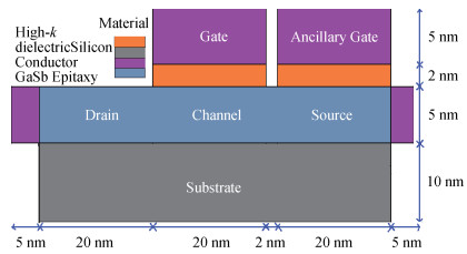
Fig. 1.
(Color online) Schematic representation of a single gate GaSb-on-Si JLTFET along with the dimensions in 2D. Width of the device is 1 μm.
SEMICONDUCTOR DEVICES
Yogesh Goswami1, , Pranav Asthana1 and Bahniman Ghosh1, 2
Corresponding author: Goswami Yogesh, Email: yogesh7692@gmail.com
Abstract: A single gate Ⅲ-Ⅴ junctionless tunnel field effect transistor (SG-JLTFET) has been reported which shows excellent dc characteristics at low power supply operation. This device has a thin uniformly n-type doped channel of GaSb i.e. gallium antimonide which is grown epitaxially over silicon substrate. The DC performance parameters such as ION, ION/IOFF, average and point subthreshold slope as well as device parameters for analog applications viz. transconductance gm, transconductance generation efficiency gm/ID, various capacitances and the unity gain frequency fT are studied using a device simulator. Along with examining its endurance to short channel effects, the performances are also compared with a Silicon Dual Gate Junctionless Tunnel FET (DG-JLTFET). The DC and small signal analog performance reflects that GaSb SG-JLTFET has immense purview for extreme high-frequency and low-power applications.
Key words: single gate junctionless tunnel field effect transistor (SG JL-TFET), gallium antimonide, band-to-band tunnelling, sub-threshold slope (SS)
| [1] |
Lilienfeld J E. Method and apparatus for controlling electric current. US Patent, 1745175, 1925 http://www.freepatentsonline.com/1745175.html
|
| [2] |
Colinge J P, Lee C W, Afzalian A, et al. Nanowire transistors without junctions. Nat Nanotechnol, 2010, 5(3): 225 doi: 10.1038/nnano.2010.15
|
| [3] |
Lee C W, Afzalian A, Akhavan N D, et al. Junctionless multigate field-effect transistor. Appl Phys Lett, 2009, 94(5): 053511 doi: 10.1063/1.3079411
|
| [4] |
Ghosh B, Mondal P, Akram M W, et al. Hetero-gate-dielectric double gate junctionless transistor (HGJLT) with reduced bandto-band tunnelling effects in subthreshold regime. J Semicond, 2013, 35(6): 064001 doi: 10.1088/1674-4926/35/6/064001/meta
|
| [5] |
Kranti A, Lee C W, Ferain I, et al. Junctionless nanowire transistor: properties and design guidelines. Proc 34th IEEE Eur Solid-State Device Res Conf, 2010: 357 http://www.sciencedirect.com/science/article/pii/S0038110111002139
|
| [6] |
Lou H J, Zhang L N, Zhu Y X, et al. A junctionless nanowire transistor with a dual-material gate. IEEE Trans Electron Devices, 2012, 59(7): 1829 doi: 10.1109/TED.2012.2192499
|
| [7] |
Lee C W, Yan R, Ferain I, et al. Nanowire zero-capacitor DRAM transistors with and without junctions. Proc 10th IEEE-NANO, 2010: 242 http://ieeexplore.ieee.org/xpl/articleDetails.jsp?arnumber=5697888
|
| [8] |
Kranti A, Lee C, Ferain I, et al. Junctionless 6T SRAM cell. IET Electron Lett, 2010, 46(22): 1491 doi: 10.1049/el.2010.2736
|
| [9] |
Choi D J, Moon D I, Kim S, et al. Nonvolatile memory by allaround-gate junctionless transistor composed of silicon nanowire on bulk substrate. IEEE Electron Device Lett, 2011, 32(5): 602 doi: 10.1109/LED.2011.2118734
|
| [10] |
Sels D, Sore B, Groeseneken G. Quantum ballistic transport in the junctionless nanowire pinch-off field effect transistor. J Comput Electron, 2010, 10(1): 216 doi: 10.1007/s10825-011-0350-2
|
| [11] |
Boucart K, Ionescu A M. Double-gate tunnel FET with high-k gate dielectric. IEEE Trans Electron Devices, 2007, 54(7): 1725 doi: 10.1109/TED.2007.899389
|
| [12] |
Boucart K, Ionescu A M. Length scaling of the double gate tunnel FET with a high-k gate dielectric. Solid-State Electron, 2007, 51(11/12): 1500 http://www.sciencedirect.com/science/article/pii/S003811010700322X
|
| [13] |
Virani H G, Adari R B R, Kottantharayil A. Dual-k spacer device architecture for the improvement of performance of silicon nchannel tunnel FETs. IEEE Trans Electron Device, 2010, 57(10): 2410 doi: 10.1109/TED.2010.2057195
|
| [14] |
Ghosh B, Akram M W. Junctionless tunnel field effect transistor. IEEE Electron Device Lett, 2013, 34(5): 584 doi: 10.1109/LED.2013.2253752
|
| [15] |
Bal P, Akram M W, Mondal P, et al. Performance estimation of sub-30 nm junctionless tunnel FET (JLTFET). J Comput Electron, 2013, 12(4): 782 doi: 10.1007/s10825-013-0483-6
|
| [16] |
Ghosh B, Bal P, Mondal P. A junctionless tunnel field effect transistor with low subthreshold slope. J Comput Electron, 2013, 12: 428 doi: 10.1007/s10825-013-0450-2
|
| [17] |
Akram M W, Ghosh B. Investigation of high performance 10-nm double gate junctionless tunnel field effect transistor. Quantum Matter, 2013, 4(6): 549 https://www.researchgate.net/publication/282626816_Investigation_of_High_Performance_10-nm_Double_Gate_Junctionless_Tunnel_Field_Effect_Transistor
|
| [18] |
Bal P, Ghosh B, Mondal P, et al. Dual material gate junctionless tunnel field effect transistor. J Comput Electron, 2014, 13(1): 230 doi: 10.1007/s10825-013-0505-4
|
| [19] |
Seo J H, Cho S, Kang I M. Simulation for silicon-compatible InGaAs-based junctionless field-effect transistor using InP buffer layer. Semicond Sci Technol, 2013, 28: 105007 doi: 10.1088/0268-1242/28/10/105007
|
| [20] |
Yoon Y J, Cho S, Seo J H, et al. Compound semiconductor tunneling field-effect transistor based on Ge/GaAs heterojunction with tunneling-boost layer for high-performance operation. Jpn J Appl Phys, 2013, 52: 04CC04 doi: 10.7567/JJAP.52.04CC04
|
| [21] |
Goswami Y, Tripathi B M M, Asthana P, et al. Junctionless tunnel field effect transistor with enhanced performance using Ⅲ-Ⅴ semiconductor. J Low Power Electron, 2013, 9: 496 doi: 10.1166/jolpe.2013.1281
|
| [22] |
Goswami Y, Ghosh B, Asthana P K. Analog performance of Si junctionless tunnel field effect transistor and its improvisation using Ⅲ-Ⅴ semiconductor. RSC Adv, 2014, 4: 10761 doi: 10.1039/c3ra46535g
|
| [23] |
Asthana P K, Ghosh N, Goswami Y, et al. High-speed and lowpower ultradeep-submicrometer Ⅲ-Ⅴ heterojunctionless tunnel field-effect transistor. IEEE Tran Electron Devices, 2014, 61(2): 479 doi: 10.1109/TED.2013.2295238
|
| [24] |
Asthana P K, Goswami Y, Ghosh N. A novel sub 20 nm single gate tunnel field effect transistor with intrinsic channel for ultra low power applications. J Semicond, 2016, 37(5): 054002 doi: 10.1088/1674-4926/37/5/054002
|
| [25] |
Akram M W, Ghosh B. Analog performance of double gate junctionless tunnel field effect transistor. J Semicond, 2014, 35(7): 074001 doi: 10.1088/1674-4926/35/7/074001
|
| [26] |
Goswami Y, Asthana P, Basak S, et al. Junctionless tunnel field effect transistor with non uniform doping. Int J Nanosci, 2015, 14: 1450025 doi: 10.1142/S0219581X14500252
|
| [27] |
Chin V W L. Electron mobility in GaSb. Solid-State Electron, 1995, 38(1): 59 doi: 10.1016/0038-1101(94)E0063-K
|
| [28] |
Podor B. Hole mobility in InP and GaSb. 31st International Spring Seminar on Electronics Technology, 2008 https://www.researchgate.net/publication/241158839_Hole_mobility_in_InP_and_GaSb
|
| [29] |
Akahane K, Yamamoto N, Gozu S, et al. Heteroepitaxial growth of GaSb on Si (001) substrates. J Cryst Growth, 2004, 264(1-3): 215 http://www.sciencedirect.com/science/article/pii/S0022024803022309
|
| [30] |
Cerutti L, Rodriguez J B, Tournie E. GaSb-based laser, monolithically grown on silicon substrate, emitting at 1.55μm at room temperature. Photonics Technol Lett, 2010, 22(8): 553 doi: 10.1109/LPT.2010.2042591
|
| [31] |
Nakamura Y, Miwa T, Ichikawa M. Nanocontact heteroepitaxy of thin GaSb and AlGaSb films on Si substrates using ultrahighdensity nanodot seeds. Nanotechnology, 2011, 22: 265301 doi: 10.1088/0957-4484/22/26/265301
|
| [32] |
Xiong K, Wang W, Zhernokletov D M, et al. Interfacial bonding and electronic structure of HfO2/GaSb interfaces: a first principles study. Appl Phys Lett, 2013, 102: 022901 doi: 10.1063/1.4775665
|
| [33] |
Tan Z, Zhao L F, Wang J, et al. Improved properties of HfO2Al2O3/GaSb MOS capacitors passivated with neutralized (NH4)2S solutions. ECS Solid State Lett, 2013, 2(8): 2162 https://www.researchgate.net/publication/270604470_Improved_properties_of_HfO2Al2O3GaSb_MOS_capacitors_passivated_with_neutralized_NH42S_solutions
|
| [34] |
Bhuwalka K K, Wang S W, Noriega O C, et al. Comparative study of high-k/GaSb interfaces for use in antimonide based MOSFETs. IEEE Electron Device Lett, 2014, 35(1): 2014 http://ieeexplore.ieee.org/document/6677541/
|
| [35] |
Robertson J. High dielectric constant oxides. Eur Phys J Appl Phys, 2004, 28(3): 265 doi: 10.1051/epjap:2004206
|
| [36] |
Documentation available at http://www.silvaco.com.
|
| [37] |
Schenk A. A model for the field and temperature dependence of SRH lifetimes in Silicon. Solid-State Electron, 1992, 35(11): 1585 doi: 10.1016/0038-1101(92)90184-E
|
| [38] |
Hansch W, Vogelsang T, Kirchner R, et al. Carrier transport near the Si/SiO2 interface of a MOSFET. Solid-State Electron, 1989, 32(10): 839 doi: 10.1016/0038-1101(89)90060-9
|


Article views: 3784 Times PDF downloads: 18 Times Cited by: 0 Times
Received: 14 September 2016 Revised: 11 November 2016 Online: Published: 01 May 2017
| Citation: |
Yogesh Goswami, Pranav Asthana, Bahniman Ghosh. Nanoscale Ⅲ-Ⅴ on Si-based junctionless tunnel transistor for EHF band applications[J]. Journal of Semiconductors, 2017, 38(5): 054002. doi: 10.1088/1674-4926/38/5/054002
****
Y Goswami, P Asthana, B Ghosh. Nanoscale Ⅲ-Ⅴ on Si-based junctionless tunnel transistor for EHF band applications[J]. J. Semicond., 2017, 38(5): 054002. doi: 10.1088/1674-4926/38/5/054002.

|
| [1] |
Lilienfeld J E. Method and apparatus for controlling electric current. US Patent, 1745175, 1925 http://www.freepatentsonline.com/1745175.html
|
| [2] |
Colinge J P, Lee C W, Afzalian A, et al. Nanowire transistors without junctions. Nat Nanotechnol, 2010, 5(3): 225 doi: 10.1038/nnano.2010.15
|
| [3] |
Lee C W, Afzalian A, Akhavan N D, et al. Junctionless multigate field-effect transistor. Appl Phys Lett, 2009, 94(5): 053511 doi: 10.1063/1.3079411
|
| [4] |
Ghosh B, Mondal P, Akram M W, et al. Hetero-gate-dielectric double gate junctionless transistor (HGJLT) with reduced bandto-band tunnelling effects in subthreshold regime. J Semicond, 2013, 35(6): 064001 doi: 10.1088/1674-4926/35/6/064001/meta
|
| [5] |
Kranti A, Lee C W, Ferain I, et al. Junctionless nanowire transistor: properties and design guidelines. Proc 34th IEEE Eur Solid-State Device Res Conf, 2010: 357 http://www.sciencedirect.com/science/article/pii/S0038110111002139
|
| [6] |
Lou H J, Zhang L N, Zhu Y X, et al. A junctionless nanowire transistor with a dual-material gate. IEEE Trans Electron Devices, 2012, 59(7): 1829 doi: 10.1109/TED.2012.2192499
|
| [7] |
Lee C W, Yan R, Ferain I, et al. Nanowire zero-capacitor DRAM transistors with and without junctions. Proc 10th IEEE-NANO, 2010: 242 http://ieeexplore.ieee.org/xpl/articleDetails.jsp?arnumber=5697888
|
| [8] |
Kranti A, Lee C, Ferain I, et al. Junctionless 6T SRAM cell. IET Electron Lett, 2010, 46(22): 1491 doi: 10.1049/el.2010.2736
|
| [9] |
Choi D J, Moon D I, Kim S, et al. Nonvolatile memory by allaround-gate junctionless transistor composed of silicon nanowire on bulk substrate. IEEE Electron Device Lett, 2011, 32(5): 602 doi: 10.1109/LED.2011.2118734
|
| [10] |
Sels D, Sore B, Groeseneken G. Quantum ballistic transport in the junctionless nanowire pinch-off field effect transistor. J Comput Electron, 2010, 10(1): 216 doi: 10.1007/s10825-011-0350-2
|
| [11] |
Boucart K, Ionescu A M. Double-gate tunnel FET with high-k gate dielectric. IEEE Trans Electron Devices, 2007, 54(7): 1725 doi: 10.1109/TED.2007.899389
|
| [12] |
Boucart K, Ionescu A M. Length scaling of the double gate tunnel FET with a high-k gate dielectric. Solid-State Electron, 2007, 51(11/12): 1500 http://www.sciencedirect.com/science/article/pii/S003811010700322X
|
| [13] |
Virani H G, Adari R B R, Kottantharayil A. Dual-k spacer device architecture for the improvement of performance of silicon nchannel tunnel FETs. IEEE Trans Electron Device, 2010, 57(10): 2410 doi: 10.1109/TED.2010.2057195
|
| [14] |
Ghosh B, Akram M W. Junctionless tunnel field effect transistor. IEEE Electron Device Lett, 2013, 34(5): 584 doi: 10.1109/LED.2013.2253752
|
| [15] |
Bal P, Akram M W, Mondal P, et al. Performance estimation of sub-30 nm junctionless tunnel FET (JLTFET). J Comput Electron, 2013, 12(4): 782 doi: 10.1007/s10825-013-0483-6
|
| [16] |
Ghosh B, Bal P, Mondal P. A junctionless tunnel field effect transistor with low subthreshold slope. J Comput Electron, 2013, 12: 428 doi: 10.1007/s10825-013-0450-2
|
| [17] |
Akram M W, Ghosh B. Investigation of high performance 10-nm double gate junctionless tunnel field effect transistor. Quantum Matter, 2013, 4(6): 549 https://www.researchgate.net/publication/282626816_Investigation_of_High_Performance_10-nm_Double_Gate_Junctionless_Tunnel_Field_Effect_Transistor
|
| [18] |
Bal P, Ghosh B, Mondal P, et al. Dual material gate junctionless tunnel field effect transistor. J Comput Electron, 2014, 13(1): 230 doi: 10.1007/s10825-013-0505-4
|
| [19] |
Seo J H, Cho S, Kang I M. Simulation for silicon-compatible InGaAs-based junctionless field-effect transistor using InP buffer layer. Semicond Sci Technol, 2013, 28: 105007 doi: 10.1088/0268-1242/28/10/105007
|
| [20] |
Yoon Y J, Cho S, Seo J H, et al. Compound semiconductor tunneling field-effect transistor based on Ge/GaAs heterojunction with tunneling-boost layer for high-performance operation. Jpn J Appl Phys, 2013, 52: 04CC04 doi: 10.7567/JJAP.52.04CC04
|
| [21] |
Goswami Y, Tripathi B M M, Asthana P, et al. Junctionless tunnel field effect transistor with enhanced performance using Ⅲ-Ⅴ semiconductor. J Low Power Electron, 2013, 9: 496 doi: 10.1166/jolpe.2013.1281
|
| [22] |
Goswami Y, Ghosh B, Asthana P K. Analog performance of Si junctionless tunnel field effect transistor and its improvisation using Ⅲ-Ⅴ semiconductor. RSC Adv, 2014, 4: 10761 doi: 10.1039/c3ra46535g
|
| [23] |
Asthana P K, Ghosh N, Goswami Y, et al. High-speed and lowpower ultradeep-submicrometer Ⅲ-Ⅴ heterojunctionless tunnel field-effect transistor. IEEE Tran Electron Devices, 2014, 61(2): 479 doi: 10.1109/TED.2013.2295238
|
| [24] |
Asthana P K, Goswami Y, Ghosh N. A novel sub 20 nm single gate tunnel field effect transistor with intrinsic channel for ultra low power applications. J Semicond, 2016, 37(5): 054002 doi: 10.1088/1674-4926/37/5/054002
|
| [25] |
Akram M W, Ghosh B. Analog performance of double gate junctionless tunnel field effect transistor. J Semicond, 2014, 35(7): 074001 doi: 10.1088/1674-4926/35/7/074001
|
| [26] |
Goswami Y, Asthana P, Basak S, et al. Junctionless tunnel field effect transistor with non uniform doping. Int J Nanosci, 2015, 14: 1450025 doi: 10.1142/S0219581X14500252
|
| [27] |
Chin V W L. Electron mobility in GaSb. Solid-State Electron, 1995, 38(1): 59 doi: 10.1016/0038-1101(94)E0063-K
|
| [28] |
Podor B. Hole mobility in InP and GaSb. 31st International Spring Seminar on Electronics Technology, 2008 https://www.researchgate.net/publication/241158839_Hole_mobility_in_InP_and_GaSb
|
| [29] |
Akahane K, Yamamoto N, Gozu S, et al. Heteroepitaxial growth of GaSb on Si (001) substrates. J Cryst Growth, 2004, 264(1-3): 215 http://www.sciencedirect.com/science/article/pii/S0022024803022309
|
| [30] |
Cerutti L, Rodriguez J B, Tournie E. GaSb-based laser, monolithically grown on silicon substrate, emitting at 1.55μm at room temperature. Photonics Technol Lett, 2010, 22(8): 553 doi: 10.1109/LPT.2010.2042591
|
| [31] |
Nakamura Y, Miwa T, Ichikawa M. Nanocontact heteroepitaxy of thin GaSb and AlGaSb films on Si substrates using ultrahighdensity nanodot seeds. Nanotechnology, 2011, 22: 265301 doi: 10.1088/0957-4484/22/26/265301
|
| [32] |
Xiong K, Wang W, Zhernokletov D M, et al. Interfacial bonding and electronic structure of HfO2/GaSb interfaces: a first principles study. Appl Phys Lett, 2013, 102: 022901 doi: 10.1063/1.4775665
|
| [33] |
Tan Z, Zhao L F, Wang J, et al. Improved properties of HfO2Al2O3/GaSb MOS capacitors passivated with neutralized (NH4)2S solutions. ECS Solid State Lett, 2013, 2(8): 2162 https://www.researchgate.net/publication/270604470_Improved_properties_of_HfO2Al2O3GaSb_MOS_capacitors_passivated_with_neutralized_NH42S_solutions
|
| [34] |
Bhuwalka K K, Wang S W, Noriega O C, et al. Comparative study of high-k/GaSb interfaces for use in antimonide based MOSFETs. IEEE Electron Device Lett, 2014, 35(1): 2014 http://ieeexplore.ieee.org/document/6677541/
|
| [35] |
Robertson J. High dielectric constant oxides. Eur Phys J Appl Phys, 2004, 28(3): 265 doi: 10.1051/epjap:2004206
|
| [36] |
Documentation available at http://www.silvaco.com.
|
| [37] |
Schenk A. A model for the field and temperature dependence of SRH lifetimes in Silicon. Solid-State Electron, 1992, 35(11): 1585 doi: 10.1016/0038-1101(92)90184-E
|
| [38] |
Hansch W, Vogelsang T, Kirchner R, et al. Carrier transport near the Si/SiO2 interface of a MOSFET. Solid-State Electron, 1989, 32(10): 839 doi: 10.1016/0038-1101(89)90060-9
|

 WeChat ID
Journal of Semiconductors © 2017 All Rights Reserved 京ICP備05085259號-2
 DownLoad:

