


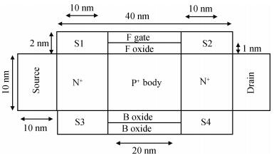
Fig. 1.
Schematic structure of an N-channel DG-MOSFET using SiGe.
SEMICONDUCTOR DEVICES
A. Singh1, , D. Kapoor1 and R. Sharma2
Corresponding author: Singh A., Email: singhakshat001.as@gmail.com
Abstract: The major purpose of this paper is to find an alternative configuration that not only minimizes the limitations of single-gate (SG) MOSFETs but also provides the better replacement for future technology. In this paper, the electrical characteristics of SiGe double-gate N-MOSFET are demonstrated and compared with electrical characteristics of Si double-gate N-MOSFET. Furthermore, in this paper the electrical characteristics of Si double-gate N-MOSFET are demonstrated and compared with electrical characteristics of Si single-gate N-MOSFET. The simulations are carried out for the device at different operational voltages using Cogenda Visual TCAD tool. Moreover, we have designed its structure and studied both Id-Vg characteristics for different voltages namely 0.05, 0.1, 0.5, 0.8, 1 and 1.5 V and Id-Vd characteristics for different voltages namely 0.1, 0.5, 1 and 1.5 V at work functions 4.5, 4.6 and 4.8 eV for this structure. The performance parameters investigated in this paper are threshold voltage, DIBL, subthreshold slope, GIDL, volume inversion and MMCR.
Key words: double gate MOSFET, DIBL, GIDL, volume inversion, SiGe, Genius tool
| [1] |
Mehrotra S R. Simulation study of silicon nanowire field effect transistors (FETs). Master of Science Dissertation, University of Delhi, 2007
|
| [2] |
Valinajad H, Hosseini R, Akbari M E. Electrical characteristics of strained double gate MOSFET. Int J Res Rev Appl Sci, 2012, 13(2): 436 http://www.arpapress.com/Volumes/Vol13Issue2/IJRRAS_13_2_07.pdf
|
| [3] |
Roy K, Mukhopadhyay S, Meimand H M. Leakage current mechanisms and reduction in techniques in deep-sub micrometer CMOS circuits. Proc IEEE, 2003, 91(2): 305 doi: 10.1109/JPROC.2002.808156
|
| [4] |
Rafhay Q, Xu C, Batude P, et al. Revisited approach for the characterization of gate induced drain leakage. Solid-State Electron, 2012, 71(1): 37 https://www.researchgate.net/publication/251998200_Revisited_approach_for_the_characterization_of_Gate_Induced_Drain_Leakage
|
| [5] |
Colinge J P. Multi-gate SOI MOSFETs. Microelectron Eng, 2007, 84(9): 2071
|
| [6] |
Mohammadi H, Abdullah H, Fu Dee C. A review on modeling the channel potential in multi-gate MOSFETs. Sains Malaysiana Publications, 2014, 43(6): 861 http://www.ukm.my/jsm/pdf_files/SM-PDF-43-6-2014/07%20Hossein%20Mohammadi.pdf
|
| [7] |
Ernst T, Cristoloveanu S, Ghibaudo G, et al. Ultimately thin double-gate SOI MOSFETs. IEEE Trans Electron Devices, 2003, 50(3): 830 doi: 10.1109/TED.2003.811371
|
| [8] |
Krishnamohan T, Jungemann C, Kim D, et al. High performance, uniaxially-strained Si and Ge, double-gate P-MOSFETs. Microelectron Eng, 2007, 84(9): 2063 http://www.academia.edu/16251397/High_Performance_Uniaxially-Strained_Silicon_and_Germanium_Double-Gate_p-MOSFETs
|
| [9] |
Mani P, Pandey M K. Silicon on insulator MOSFET development from single-gate to multiple-gate. Int J Adv Res Comput Sci Softw Eng, 2012, 2(6): 297 https://www.researchgate.net/profile/Prashant_Yadav6/publication/276415747_Silicon_on_Insulator_MOSFET_Development_from_Single_Gate_to_Multiple_Gate/links/55f7dbc408aeafc8ac06a331.pdf?inViewer=true&disableCoverPage=true&origin=publication_detail
|
| [10] |
Dubey S, Tiwari P K, Jit S. On-current modeling of short-channel double-gate (DG) MOSFETs with a vertical Gaussian-like doping profile. J Semicond, 2013, 34(5): 1 http://www.oalib.com/paper/1521617
|
| [11] |
Subramaniam S, Wale R N A, Joshi S M. Drain current models for single-gate MOSFETs and undoped symmetric and asymmetric double-gate SOI MOSFETs and quantum mechanical effects: a review. Int J Eng Sci Technol, 2013, 5(1): 96 http://www.oalib.com/paper/2096893
|
| [12] |
Wagner M. Simulation of thermoelectric devices. Doctorate of Philosophy Dissertation, Vienna University of Technology, 2007
|
| [13] |
Kim D. Theoretical performance evaluations of N MOS double gate FETs with high mobility material: strained Ⅲ-Ⅴ, Ge and Si. Doctorate of Philosophy Dissertation Stanford University, 2009
|
| [14] |
Sahu D, Tirkey A. Design and simulation of double gate FETs using ATLAS. Bachelors of Technology Project, National Institute of Technology, Rourkela, 2014
|
| [15] |
Singh A, Kapoor D, Sharma R. Review of SiGe double gate N-MOSFET. Int J Inform Technol Syst, 2015, 4(1): 19 http://www.academia.edu/14426107/Review_of_SiGe_Double_Gate_N-MOSFET
|
| [16] |
Loke A, Wu Z Y, Moallemi R, et al. Constant-current threshold voltage extraction in HSPICE for nanoscale CMOS analog design. Synopsys Users Group (SNUG): Advanced Micro Devices Inc. , Third Edition, 2010
|
| [17] |
Boucart K, Ionescu A M. Double-gate tunnel FE T with high-gate dielectric. IEEE Trans Electron Devices, 2007, 54(7): 17 https://www.researchgate.net/profile/Adrian_Ionescu/publication/47696037_Length_scaling_of_the_Double_Gate_Tunnel_FET_with_a_high-K_gate_dielectric/links/54a929240cf2eecc56e56e10.pdf?origin=publication_list
|
| [18] |
Sharma R. Analytical modeling of volume inversion and channel length modulation in fully depleted double gate nanoscale SOI MOSFETs. J Electron Devices, 2013, 18(2): 1553 http://jeldev.org/18_Rajiv%20Sharma.pdf
|
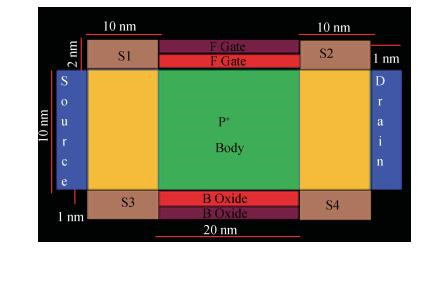
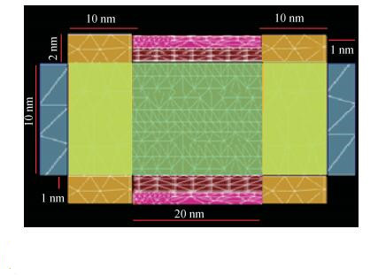
Table 1. Various parameters used in N-channel DG-MOSFET using SiGe.

|
Table 2. Comparison between various parameters used in N-channel DG-MOSFET using SiGe and N-channel DG-MOSFET using Si.

|
Table 3. Comparison between various parameters used in N-channel SG-MOSFET using Si and N-channel DG-MOSFET using Si.

|
| [1] |
Mehrotra S R. Simulation study of silicon nanowire field effect transistors (FETs). Master of Science Dissertation, University of Delhi, 2007
|
| [2] |
Valinajad H, Hosseini R, Akbari M E. Electrical characteristics of strained double gate MOSFET. Int J Res Rev Appl Sci, 2012, 13(2): 436 http://www.arpapress.com/Volumes/Vol13Issue2/IJRRAS_13_2_07.pdf
|
| [3] |
Roy K, Mukhopadhyay S, Meimand H M. Leakage current mechanisms and reduction in techniques in deep-sub micrometer CMOS circuits. Proc IEEE, 2003, 91(2): 305 doi: 10.1109/JPROC.2002.808156
|
| [4] |
Rafhay Q, Xu C, Batude P, et al. Revisited approach for the characterization of gate induced drain leakage. Solid-State Electron, 2012, 71(1): 37 https://www.researchgate.net/publication/251998200_Revisited_approach_for_the_characterization_of_Gate_Induced_Drain_Leakage
|
| [5] |
Colinge J P. Multi-gate SOI MOSFETs. Microelectron Eng, 2007, 84(9): 2071
|
| [6] |
Mohammadi H, Abdullah H, Fu Dee C. A review on modeling the channel potential in multi-gate MOSFETs. Sains Malaysiana Publications, 2014, 43(6): 861 http://www.ukm.my/jsm/pdf_files/SM-PDF-43-6-2014/07%20Hossein%20Mohammadi.pdf
|
| [7] |
Ernst T, Cristoloveanu S, Ghibaudo G, et al. Ultimately thin double-gate SOI MOSFETs. IEEE Trans Electron Devices, 2003, 50(3): 830 doi: 10.1109/TED.2003.811371
|
| [8] |
Krishnamohan T, Jungemann C, Kim D, et al. High performance, uniaxially-strained Si and Ge, double-gate P-MOSFETs. Microelectron Eng, 2007, 84(9): 2063 http://www.academia.edu/16251397/High_Performance_Uniaxially-Strained_Silicon_and_Germanium_Double-Gate_p-MOSFETs
|
| [9] |
Mani P, Pandey M K. Silicon on insulator MOSFET development from single-gate to multiple-gate. Int J Adv Res Comput Sci Softw Eng, 2012, 2(6): 297 https://www.researchgate.net/profile/Prashant_Yadav6/publication/276415747_Silicon_on_Insulator_MOSFET_Development_from_Single_Gate_to_Multiple_Gate/links/55f7dbc408aeafc8ac06a331.pdf?inViewer=true&disableCoverPage=true&origin=publication_detail
|
| [10] |
Dubey S, Tiwari P K, Jit S. On-current modeling of short-channel double-gate (DG) MOSFETs with a vertical Gaussian-like doping profile. J Semicond, 2013, 34(5): 1 http://www.oalib.com/paper/1521617
|
| [11] |
Subramaniam S, Wale R N A, Joshi S M. Drain current models for single-gate MOSFETs and undoped symmetric and asymmetric double-gate SOI MOSFETs and quantum mechanical effects: a review. Int J Eng Sci Technol, 2013, 5(1): 96 http://www.oalib.com/paper/2096893
|
| [12] |
Wagner M. Simulation of thermoelectric devices. Doctorate of Philosophy Dissertation, Vienna University of Technology, 2007
|
| [13] |
Kim D. Theoretical performance evaluations of N MOS double gate FETs with high mobility material: strained Ⅲ-Ⅴ, Ge and Si. Doctorate of Philosophy Dissertation Stanford University, 2009
|
| [14] |
Sahu D, Tirkey A. Design and simulation of double gate FETs using ATLAS. Bachelors of Technology Project, National Institute of Technology, Rourkela, 2014
|
| [15] |
Singh A, Kapoor D, Sharma R. Review of SiGe double gate N-MOSFET. Int J Inform Technol Syst, 2015, 4(1): 19 http://www.academia.edu/14426107/Review_of_SiGe_Double_Gate_N-MOSFET
|
| [16] |
Loke A, Wu Z Y, Moallemi R, et al. Constant-current threshold voltage extraction in HSPICE for nanoscale CMOS analog design. Synopsys Users Group (SNUG): Advanced Micro Devices Inc. , Third Edition, 2010
|
| [17] |
Boucart K, Ionescu A M. Double-gate tunnel FE T with high-gate dielectric. IEEE Trans Electron Devices, 2007, 54(7): 17 https://www.researchgate.net/profile/Adrian_Ionescu/publication/47696037_Length_scaling_of_the_Double_Gate_Tunnel_FET_with_a_high-K_gate_dielectric/links/54a929240cf2eecc56e56e10.pdf?origin=publication_list
|
| [18] |
Sharma R. Analytical modeling of volume inversion and channel length modulation in fully depleted double gate nanoscale SOI MOSFETs. J Electron Devices, 2013, 18(2): 1553 http://jeldev.org/18_Rajiv%20Sharma.pdf
|


Article views: 5156 Times PDF downloads: 75 Times Cited by: 0 Times
Received: 01 July 2016 Revised: 26 October 2016 Online: Published: 01 April 2017
| Citation: |
A. Singh, D. Kapoor, R. Sharma. Performance analysis of SiGe double-gate N-MOSFET[J]. Journal of Semiconductors, 2017, 38(4): 044003. doi: 10.1088/1674-4926/38/4/044003
****
A Singh, D Kapoor, R Sharma. Performance analysis of SiGe double-gate N-MOSFET[J]. J. Semicond., 2017, 38(4): 044003. doi:? 10.1088/1674-4926/38/4/044003.

|
| [1] |
Mehrotra S R. Simulation study of silicon nanowire field effect transistors (FETs). Master of Science Dissertation, University of Delhi, 2007
|
| [2] |
Valinajad H, Hosseini R, Akbari M E. Electrical characteristics of strained double gate MOSFET. Int J Res Rev Appl Sci, 2012, 13(2): 436 http://www.arpapress.com/Volumes/Vol13Issue2/IJRRAS_13_2_07.pdf
|
| [3] |
Roy K, Mukhopadhyay S, Meimand H M. Leakage current mechanisms and reduction in techniques in deep-sub micrometer CMOS circuits. Proc IEEE, 2003, 91(2): 305 doi: 10.1109/JPROC.2002.808156
|
| [4] |
Rafhay Q, Xu C, Batude P, et al. Revisited approach for the characterization of gate induced drain leakage. Solid-State Electron, 2012, 71(1): 37 https://www.researchgate.net/publication/251998200_Revisited_approach_for_the_characterization_of_Gate_Induced_Drain_Leakage
|
| [5] |
Colinge J P. Multi-gate SOI MOSFETs. Microelectron Eng, 2007, 84(9): 2071
|
| [6] |
Mohammadi H, Abdullah H, Fu Dee C. A review on modeling the channel potential in multi-gate MOSFETs. Sains Malaysiana Publications, 2014, 43(6): 861 http://www.ukm.my/jsm/pdf_files/SM-PDF-43-6-2014/07%20Hossein%20Mohammadi.pdf
|
| [7] |
Ernst T, Cristoloveanu S, Ghibaudo G, et al. Ultimately thin double-gate SOI MOSFETs. IEEE Trans Electron Devices, 2003, 50(3): 830 doi: 10.1109/TED.2003.811371
|
| [8] |
Krishnamohan T, Jungemann C, Kim D, et al. High performance, uniaxially-strained Si and Ge, double-gate P-MOSFETs. Microelectron Eng, 2007, 84(9): 2063 http://www.academia.edu/16251397/High_Performance_Uniaxially-Strained_Silicon_and_Germanium_Double-Gate_p-MOSFETs
|
| [9] |
Mani P, Pandey M K. Silicon on insulator MOSFET development from single-gate to multiple-gate. Int J Adv Res Comput Sci Softw Eng, 2012, 2(6): 297 https://www.researchgate.net/profile/Prashant_Yadav6/publication/276415747_Silicon_on_Insulator_MOSFET_Development_from_Single_Gate_to_Multiple_Gate/links/55f7dbc408aeafc8ac06a331.pdf?inViewer=true&disableCoverPage=true&origin=publication_detail
|
| [10] |
Dubey S, Tiwari P K, Jit S. On-current modeling of short-channel double-gate (DG) MOSFETs with a vertical Gaussian-like doping profile. J Semicond, 2013, 34(5): 1 http://www.oalib.com/paper/1521617
|
| [11] |
Subramaniam S, Wale R N A, Joshi S M. Drain current models for single-gate MOSFETs and undoped symmetric and asymmetric double-gate SOI MOSFETs and quantum mechanical effects: a review. Int J Eng Sci Technol, 2013, 5(1): 96 http://www.oalib.com/paper/2096893
|
| [12] |
Wagner M. Simulation of thermoelectric devices. Doctorate of Philosophy Dissertation, Vienna University of Technology, 2007
|
| [13] |
Kim D. Theoretical performance evaluations of N MOS double gate FETs with high mobility material: strained Ⅲ-Ⅴ, Ge and Si. Doctorate of Philosophy Dissertation Stanford University, 2009
|
| [14] |
Sahu D, Tirkey A. Design and simulation of double gate FETs using ATLAS. Bachelors of Technology Project, National Institute of Technology, Rourkela, 2014
|
| [15] |
Singh A, Kapoor D, Sharma R. Review of SiGe double gate N-MOSFET. Int J Inform Technol Syst, 2015, 4(1): 19 http://www.academia.edu/14426107/Review_of_SiGe_Double_Gate_N-MOSFET
|
| [16] |
Loke A, Wu Z Y, Moallemi R, et al. Constant-current threshold voltage extraction in HSPICE for nanoscale CMOS analog design. Synopsys Users Group (SNUG): Advanced Micro Devices Inc. , Third Edition, 2010
|
| [17] |
Boucart K, Ionescu A M. Double-gate tunnel FE T with high-gate dielectric. IEEE Trans Electron Devices, 2007, 54(7): 17 https://www.researchgate.net/profile/Adrian_Ionescu/publication/47696037_Length_scaling_of_the_Double_Gate_Tunnel_FET_with_a_high-K_gate_dielectric/links/54a929240cf2eecc56e56e10.pdf?origin=publication_list
|
| [18] |
Sharma R. Analytical modeling of volume inversion and channel length modulation in fully depleted double gate nanoscale SOI MOSFETs. J Electron Devices, 2013, 18(2): 1553 http://jeldev.org/18_Rajiv%20Sharma.pdf
|

 WeChat ID
Journal of Semiconductors © 2017 All Rights Reserved 京ICP備05085259號(hào)-2
 DownLoad:

