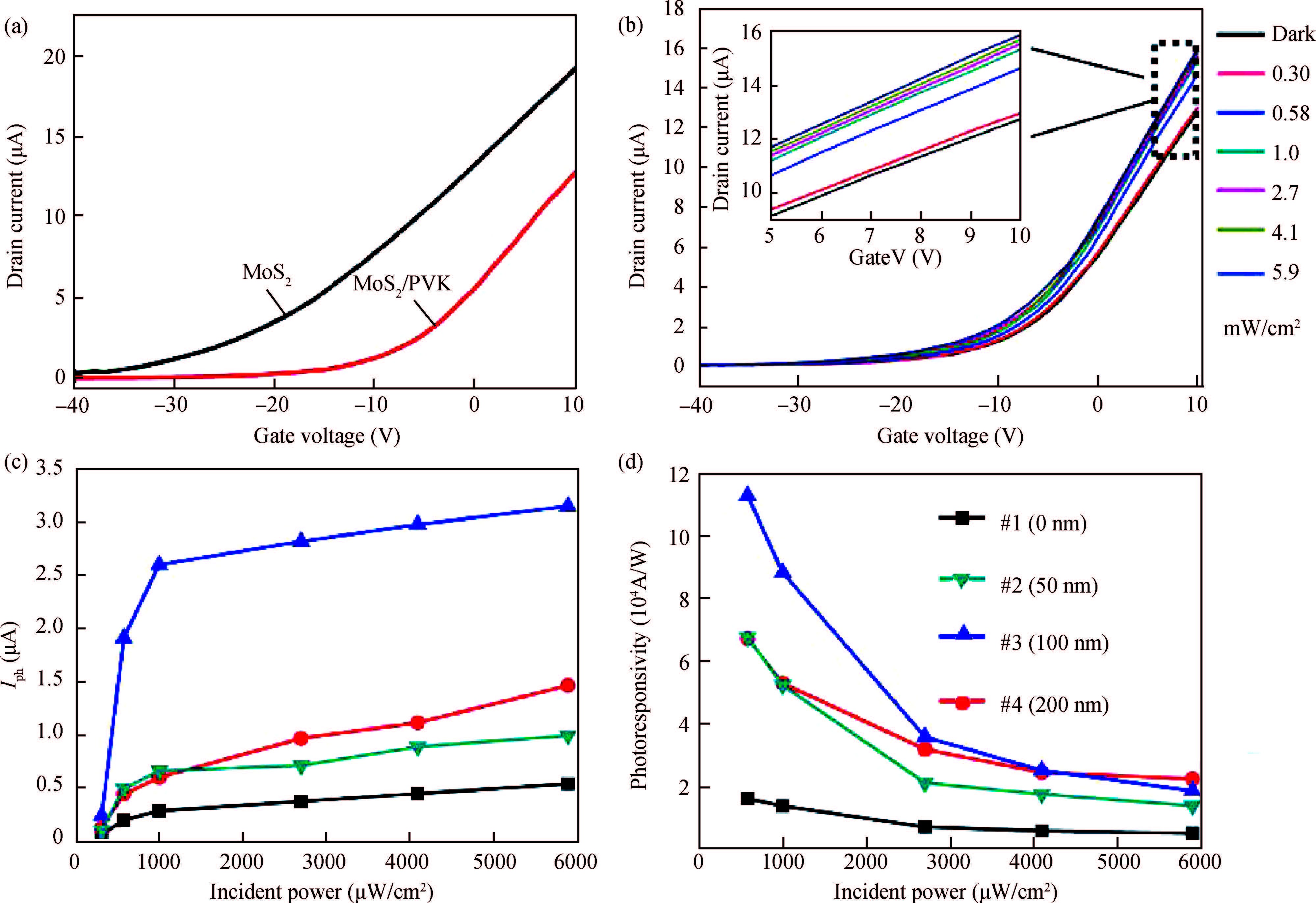
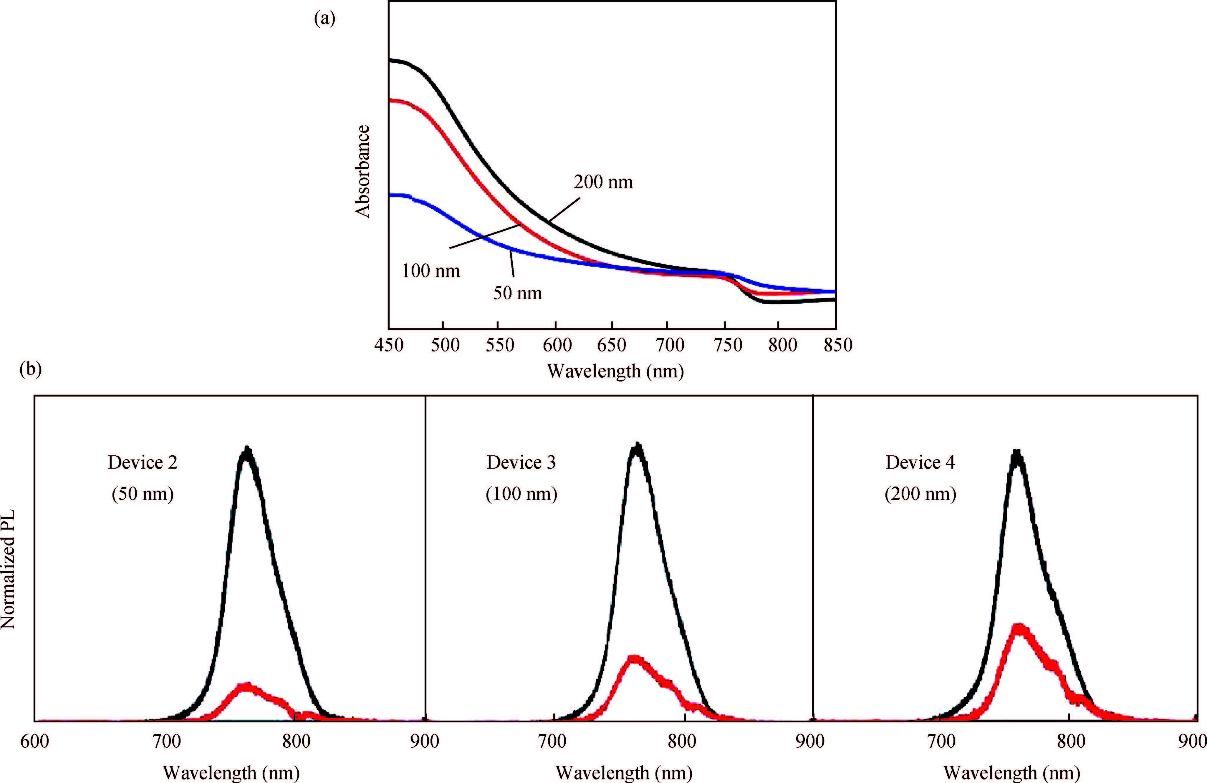
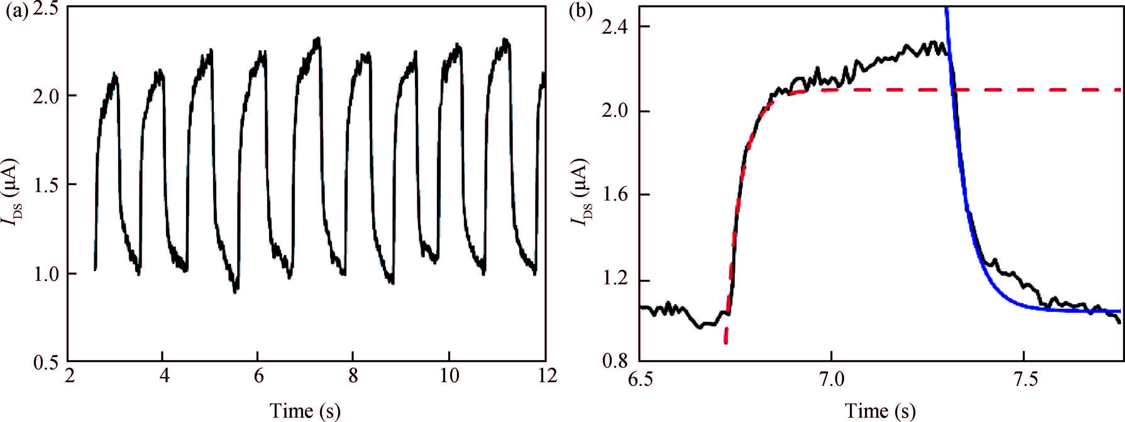
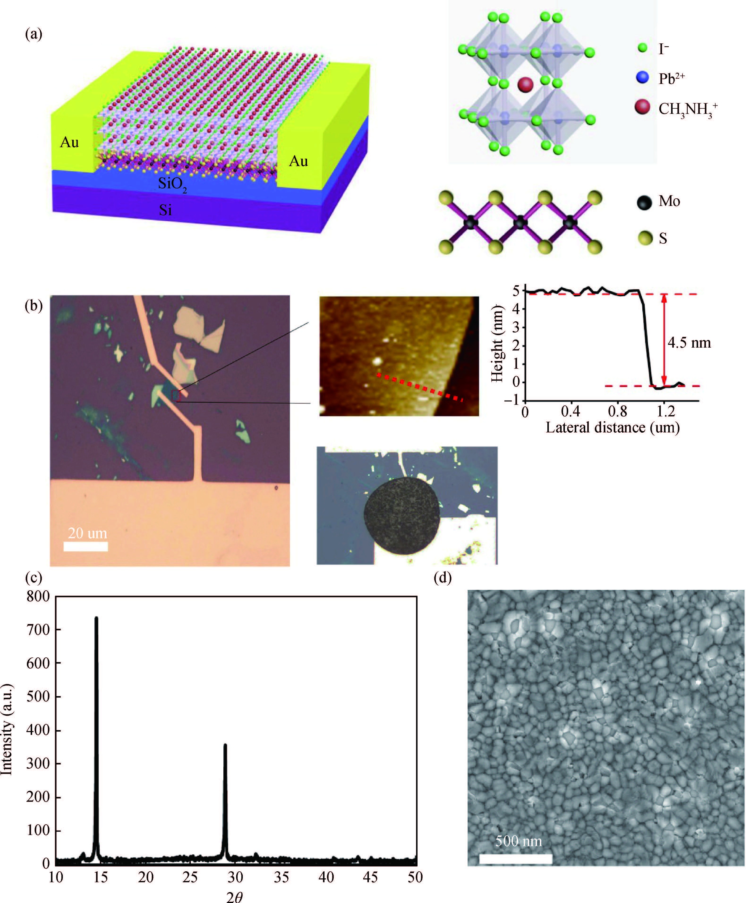
SPECIAL TOPIC ON 2D MATERIALS AND DEVICES
Fengjing Liu1, 2, Jiawei Wang2, Liang Wang2, Xiaoyong Cai2, Chao Jiang2, and Gongtang Wang1,
Corresponding author: Chao Jiang, Email:Jiangch@nanoctr.cn; Gongtang Wang,Email:wanggt@sdnu.edu.cn
Abstract: Perovskite/MoS2 hybrid thin film transistor photodetectors consist of few-layered MoS2 and CH3NH3PbI3 film with various thickness prepared by two-step vacuum deposition. By implementing perovskite CH3NH3PbI3 film onto the MoS2 flake, the perovskite/MoS2 hybrid photodetector exhibited a photoresponsivity of 104A/W and fast response time of about 40 ms. Improvement of photodetection performance is attributed to the balance between light absorption in the perovskite layer and an effective transfer of photogenerated carriers from perovskite entering the MoS2 channel. This work may provide guidance to develop high-performance hybrid structure optoelectronic devices.
Key words: perovskite, MoS2, photodetector
| [1] |
Sangwan V K, Jariwala D, Kim I S, et al. Gate-tunable memristive phenomena mediated by grain boundaries in single-layer MoS2. Nat Nanotech, 2015, 10(5):403 doi: 10.1038/nnano.2015.56
|
| [2] |
Lopez-Sanchez O, Lembke D, Kayci M, et al. Ultrasensitive photodetectors based on monolayer MoS2. Nat Nanotech, 2013, 8(7):497 doi: 10.1038/nnano.2013.100
|
| [3] |
Gong Y J, Lin J H, Wang X L, et al. Vertical and in-plane heterostructures from WS2/MoS2 monolayers. Nat Mater, 2014, 13(12):1135 doi: 10.1038/nmat4091
|
| [4] |
Liu Y, Weiss N O, Duan X, et al. Van der Waals heterostructures and devices. Nat Rev Mater, 2016:16042
|
| [5] |
Li X, Lin M W, Lin J, et al. Two-dimensional GaSe/MoSe2 misfit bilayer heterojunctions by van der Waals epitaxy. Sci Adv, 2016, 2(4):e1501882 https://www.ornl.gov/content/two-dimensional-gasemose2-misfit-bilayer-heterojunctions-van-der-waals-epitaxy
|
| [6] |
Kim S, Konar A, Hwang W S, et al. High-mobility and lowpower thin-film transistors based on multilayer MoS2 crystals. Nat Commun, 2012, 3:1011 doi: 10.1038/ncomms2018
|
| [7] |
Lopez-Sanchez O, Lembke D, Kayci M, et al. Ultrasensitive photodetectors based on monolayer MoS2. Nat Nanotech, 2013, 8(7):497 doi: 10.1038/nnano.2013.100
|
| [8] |
Choi W, Cho M Y, Konar A, et al. High-detectivity multilayer MoS2 phototransistors with spectral response from ultraviolet to infrared. Adv Mater, 2012, 24(43):5832 doi: 10.1002/adma.201201909
|
| [9] |
Yu S H, Lee Y, Jang S K, et al. Dye-sensitized MoS2 photodetector with enhanced spectral photoresponse. ACS Nano, 2014, 8(8):8285 doi: 10.1021/nn502715h
|
| [10] |
Pak J, Jang J, Cho K, et al. Enhancement of photodetection characteristics of MoS2 field effect transistors using surface treatment with copper phthalocyanine. Nanoscale, 2015, 7(44):18780 doi: 10.1039/C5NR04836B
|
| [11] |
Kufer D, Nikitskiy I, Lasanta T, et al. Hybrid 2D-0D MoS2-PbS quantum dot photodetectors. Adv Mater, 2015, 27(1):176 doi: 10.1002/adma.v27.1
|
| [12] |
Kazim S, Nazeeruddin M K, Gratzel M, et al. Perovskite as light harvester:a game changer in photovoltaics. Angew Chem Int Edit, 2014, 53(11):2812 doi: 10.1002/anie.v53.11
|
| [13] |
Kim H S, Lee C R, Im J H, et al. Lead Iodide perovskite sensitized all-solid-state submicron thin film mesoscopic solar cell with efficiency exceeding 9%. Sci Rep, 2012, 2:7 https://www.researchgate.net/profile/Jacques-E_Moser/publication/230716542_Lead_Iodide_Perovskite_Sensitized_All-Solid-State_Submicron_Thin_Film_Mesoscopic_Solar_Cell_with_Efficiency_Exceeding_9/links/09e41506f09cb81b07000000.pdf?origin=publication_detail
|
| [14] |
Yang W S, Noh J H, Jeon N J, et al. High-performance photovoltaic perovskite layers fabricated through intramolecular exchange. Science, 2015, 348(6240):1234 doi: 10.1126/science.aaa9272
|
| [15] |
Lee Y, Kwon J, Hwang E, et al. High-performance perovskitegraphene hybrid photodetector. Adv Mater, 2015, 27(1):41 doi: 10.1002/adma.v27.1
|
| [16] |
Kwak D H, Lim D H, Ra H S, et al. High performance hybrid graphene-CsPbBr3-xIx perovskite nanocrystal photodetector. RSC Adv, 2016, 6(69):65252 doi: 10.1039/C6RA08699C
|
| [17] |
Ma C, Shi Y M, Hu W J, et al. Heterostructured WS2/CH3NH3PbI3 photoconductors with suppressed dark current and enhanced photodetectivity. Adv Mater, 2016, 28(19):3683 doi: 10.1002/adma.v28.19
|
| [18] |
Radisavljevic B, Radenovic A, Brivio J, et al. Single-layer MoS2 transistors. Nat Nanotech, 2011, 6(3):147 doi: 10.1038/nnano.2010.279
|
| [19] |
Shkrob I A, Marin T W. Charge trapping in photovoltaically active perovskites and related halogenoplumbate compounds. J Phys Chem Lett, 2014, 5(7):1066 doi: 10.1021/jz5004022
|
| [20] |
Kim J, Lee S H, Lee J H, et al. The role of intrinsic defects in methylammonium lead iodide perovskite. J Phys Chem Lett, 2014, 5(8):1312 doi: 10.1021/jz500370k
|
| [21] |
Dong R, Fang Y, Chae J, et al. High-gain and low-driving-voltage photodetectors based on organolead triiodide perovskites. Adv Mater, 2015, 27(11):1912 doi: 10.1002/adma.v27.11
|
| [22] |
Zhang H, Cheng J Q, Lin F, et al. Pinhole-free and surfacenanostructured niox film by room-temperature solution process for high-performance flexible perovskite solar cells with good stability and reproducibility. ACS Nano, 2016, 10(1):1503 doi: 10.1021/acsnano.5b07043
|
Table 1. Summary of the thickness and electrical properties of MoS2 FETs.
| Device | PbI2 thickness(nm) | Mobility(cm2V-1s-1) | Responsivity (A/W) |
| #1 | 0 | 19.7 | 1.5×10³ |
| #2 | 50 | 20.4 | 6.6×10³ |
| #3 | 100 | 19.7 | 1.1×10⁴ |
| #4 | 200 | 20.3 | 6.7×10³ |
DownLoad: CSV
| [1] |
Sangwan V K, Jariwala D, Kim I S, et al. Gate-tunable memristive phenomena mediated by grain boundaries in single-layer MoS2. Nat Nanotech, 2015, 10(5):403 doi: 10.1038/nnano.2015.56
|
| [2] |
Lopez-Sanchez O, Lembke D, Kayci M, et al. Ultrasensitive photodetectors based on monolayer MoS2. Nat Nanotech, 2013, 8(7):497 doi: 10.1038/nnano.2013.100
|
| [3] |
Gong Y J, Lin J H, Wang X L, et al. Vertical and in-plane heterostructures from WS2/MoS2 monolayers. Nat Mater, 2014, 13(12):1135 doi: 10.1038/nmat4091
|
| [4] |
Liu Y, Weiss N O, Duan X, et al. Van der Waals heterostructures and devices. Nat Rev Mater, 2016:16042
|
| [5] |
Li X, Lin M W, Lin J, et al. Two-dimensional GaSe/MoSe2 misfit bilayer heterojunctions by van der Waals epitaxy. Sci Adv, 2016, 2(4):e1501882 https://www.ornl.gov/content/two-dimensional-gasemose2-misfit-bilayer-heterojunctions-van-der-waals-epitaxy
|
| [6] |
Kim S, Konar A, Hwang W S, et al. High-mobility and lowpower thin-film transistors based on multilayer MoS2 crystals. Nat Commun, 2012, 3:1011 doi: 10.1038/ncomms2018
|
| [7] |
Lopez-Sanchez O, Lembke D, Kayci M, et al. Ultrasensitive photodetectors based on monolayer MoS2. Nat Nanotech, 2013, 8(7):497 doi: 10.1038/nnano.2013.100
|
| [8] |
Choi W, Cho M Y, Konar A, et al. High-detectivity multilayer MoS2 phototransistors with spectral response from ultraviolet to infrared. Adv Mater, 2012, 24(43):5832 doi: 10.1002/adma.201201909
|
| [9] |
Yu S H, Lee Y, Jang S K, et al. Dye-sensitized MoS2 photodetector with enhanced spectral photoresponse. ACS Nano, 2014, 8(8):8285 doi: 10.1021/nn502715h
|
| [10] |
Pak J, Jang J, Cho K, et al. Enhancement of photodetection characteristics of MoS2 field effect transistors using surface treatment with copper phthalocyanine. Nanoscale, 2015, 7(44):18780 doi: 10.1039/C5NR04836B
|
| [11] |
Kufer D, Nikitskiy I, Lasanta T, et al. Hybrid 2D-0D MoS2-PbS quantum dot photodetectors. Adv Mater, 2015, 27(1):176 doi: 10.1002/adma.v27.1
|
| [12] |
Kazim S, Nazeeruddin M K, Gratzel M, et al. Perovskite as light harvester:a game changer in photovoltaics. Angew Chem Int Edit, 2014, 53(11):2812 doi: 10.1002/anie.v53.11
|
| [13] |
Kim H S, Lee C R, Im J H, et al. Lead Iodide perovskite sensitized all-solid-state submicron thin film mesoscopic solar cell with efficiency exceeding 9%. Sci Rep, 2012, 2:7 https://www.researchgate.net/profile/Jacques-E_Moser/publication/230716542_Lead_Iodide_Perovskite_Sensitized_All-Solid-State_Submicron_Thin_Film_Mesoscopic_Solar_Cell_with_Efficiency_Exceeding_9/links/09e41506f09cb81b07000000.pdf?origin=publication_detail
|
| [14] |
Yang W S, Noh J H, Jeon N J, et al. High-performance photovoltaic perovskite layers fabricated through intramolecular exchange. Science, 2015, 348(6240):1234 doi: 10.1126/science.aaa9272
|
| [15] |
Lee Y, Kwon J, Hwang E, et al. High-performance perovskitegraphene hybrid photodetector. Adv Mater, 2015, 27(1):41 doi: 10.1002/adma.v27.1
|
| [16] |
Kwak D H, Lim D H, Ra H S, et al. High performance hybrid graphene-CsPbBr3-xIx perovskite nanocrystal photodetector. RSC Adv, 2016, 6(69):65252 doi: 10.1039/C6RA08699C
|
| [17] |
Ma C, Shi Y M, Hu W J, et al. Heterostructured WS2/CH3NH3PbI3 photoconductors with suppressed dark current and enhanced photodetectivity. Adv Mater, 2016, 28(19):3683 doi: 10.1002/adma.v28.19
|
| [18] |
Radisavljevic B, Radenovic A, Brivio J, et al. Single-layer MoS2 transistors. Nat Nanotech, 2011, 6(3):147 doi: 10.1038/nnano.2010.279
|
| [19] |
Shkrob I A, Marin T W. Charge trapping in photovoltaically active perovskites and related halogenoplumbate compounds. J Phys Chem Lett, 2014, 5(7):1066 doi: 10.1021/jz5004022
|
| [20] |
Kim J, Lee S H, Lee J H, et al. The role of intrinsic defects in methylammonium lead iodide perovskite. J Phys Chem Lett, 2014, 5(8):1312 doi: 10.1021/jz500370k
|
| [21] |
Dong R, Fang Y, Chae J, et al. High-gain and low-driving-voltage photodetectors based on organolead triiodide perovskites. Adv Mater, 2015, 27(11):1912 doi: 10.1002/adma.v27.11
|
| [22] |
Zhang H, Cheng J Q, Lin F, et al. Pinhole-free and surfacenanostructured niox film by room-temperature solution process for high-performance flexible perovskite solar cells with good stability and reproducibility. ACS Nano, 2016, 10(1):1503 doi: 10.1021/acsnano.5b07043
|
Article views: 6197 Times PDF downloads: 50 Times Cited by: 0 Times
Received: 07 November 2016 Revised: 30 November 2016 Online: Published: 01 March 2017
| Citation: |
Fengjing Liu, Jiawei Wang, Liang Wang, Xiaoyong Cai, Chao Jiang, Gongtang Wang. Enhancement of photodetection based on perovskite/MoS2 hybrid thin film transistor[J]. Journal of Semiconductors, 2017, 38(3): 034002. doi: 10.1088/1674-4926/38/3/034002
****
F J Liu, J W Wang, L Wang, X Y Cai, C Jiang, G T Wang. Enhancement of photodetection based on perovskite/MoS2 hybrid thin film transistor[J]. J. Semicond., 2017, 38(3): 034002. doi: 10.1088/1674-4926/38/3/034002.
|
Project supported by the National Natural Science Foundation of China (Nos.11374070,61327009 214320051) and the Strategic Priority Research Program of the Chinese Academy of Sciences (No.XDA09040201)
the Strategic Priority Research Program of the Chinese Academy of Sciences No.XDA09040201
Project supported by the National Natural Science Foundation of China Nos.11374070,61327009 214320051
| [1] |
Sangwan V K, Jariwala D, Kim I S, et al. Gate-tunable memristive phenomena mediated by grain boundaries in single-layer MoS2. Nat Nanotech, 2015, 10(5):403 doi: 10.1038/nnano.2015.56
|
| [2] |
Lopez-Sanchez O, Lembke D, Kayci M, et al. Ultrasensitive photodetectors based on monolayer MoS2. Nat Nanotech, 2013, 8(7):497 doi: 10.1038/nnano.2013.100
|
| [3] |
Gong Y J, Lin J H, Wang X L, et al. Vertical and in-plane heterostructures from WS2/MoS2 monolayers. Nat Mater, 2014, 13(12):1135 doi: 10.1038/nmat4091
|
| [4] |
Liu Y, Weiss N O, Duan X, et al. Van der Waals heterostructures and devices. Nat Rev Mater, 2016:16042
|
| [5] |
Li X, Lin M W, Lin J, et al. Two-dimensional GaSe/MoSe2 misfit bilayer heterojunctions by van der Waals epitaxy. Sci Adv, 2016, 2(4):e1501882 https://www.ornl.gov/content/two-dimensional-gasemose2-misfit-bilayer-heterojunctions-van-der-waals-epitaxy
|
| [6] |
Kim S, Konar A, Hwang W S, et al. High-mobility and lowpower thin-film transistors based on multilayer MoS2 crystals. Nat Commun, 2012, 3:1011 doi: 10.1038/ncomms2018
|
| [7] |
Lopez-Sanchez O, Lembke D, Kayci M, et al. Ultrasensitive photodetectors based on monolayer MoS2. Nat Nanotech, 2013, 8(7):497 doi: 10.1038/nnano.2013.100
|
| [8] |
Choi W, Cho M Y, Konar A, et al. High-detectivity multilayer MoS2 phototransistors with spectral response from ultraviolet to infrared. Adv Mater, 2012, 24(43):5832 doi: 10.1002/adma.201201909
|
| [9] |
Yu S H, Lee Y, Jang S K, et al. Dye-sensitized MoS2 photodetector with enhanced spectral photoresponse. ACS Nano, 2014, 8(8):8285 doi: 10.1021/nn502715h
|
| [10] |
Pak J, Jang J, Cho K, et al. Enhancement of photodetection characteristics of MoS2 field effect transistors using surface treatment with copper phthalocyanine. Nanoscale, 2015, 7(44):18780 doi: 10.1039/C5NR04836B
|
| [11] |
Kufer D, Nikitskiy I, Lasanta T, et al. Hybrid 2D-0D MoS2-PbS quantum dot photodetectors. Adv Mater, 2015, 27(1):176 doi: 10.1002/adma.v27.1
|
| [12] |
Kazim S, Nazeeruddin M K, Gratzel M, et al. Perovskite as light harvester:a game changer in photovoltaics. Angew Chem Int Edit, 2014, 53(11):2812 doi: 10.1002/anie.v53.11
|
| [13] |
Kim H S, Lee C R, Im J H, et al. Lead Iodide perovskite sensitized all-solid-state submicron thin film mesoscopic solar cell with efficiency exceeding 9%. Sci Rep, 2012, 2:7 https://www.researchgate.net/profile/Jacques-E_Moser/publication/230716542_Lead_Iodide_Perovskite_Sensitized_All-Solid-State_Submicron_Thin_Film_Mesoscopic_Solar_Cell_with_Efficiency_Exceeding_9/links/09e41506f09cb81b07000000.pdf?origin=publication_detail
|
| [14] |
Yang W S, Noh J H, Jeon N J, et al. High-performance photovoltaic perovskite layers fabricated through intramolecular exchange. Science, 2015, 348(6240):1234 doi: 10.1126/science.aaa9272
|
| [15] |
Lee Y, Kwon J, Hwang E, et al. High-performance perovskitegraphene hybrid photodetector. Adv Mater, 2015, 27(1):41 doi: 10.1002/adma.v27.1
|
| [16] |
Kwak D H, Lim D H, Ra H S, et al. High performance hybrid graphene-CsPbBr3-xIx perovskite nanocrystal photodetector. RSC Adv, 2016, 6(69):65252 doi: 10.1039/C6RA08699C
|
| [17] |
Ma C, Shi Y M, Hu W J, et al. Heterostructured WS2/CH3NH3PbI3 photoconductors with suppressed dark current and enhanced photodetectivity. Adv Mater, 2016, 28(19):3683 doi: 10.1002/adma.v28.19
|
| [18] |
Radisavljevic B, Radenovic A, Brivio J, et al. Single-layer MoS2 transistors. Nat Nanotech, 2011, 6(3):147 doi: 10.1038/nnano.2010.279
|
| [19] |
Shkrob I A, Marin T W. Charge trapping in photovoltaically active perovskites and related halogenoplumbate compounds. J Phys Chem Lett, 2014, 5(7):1066 doi: 10.1021/jz5004022
|
| [20] |
Kim J, Lee S H, Lee J H, et al. The role of intrinsic defects in methylammonium lead iodide perovskite. J Phys Chem Lett, 2014, 5(8):1312 doi: 10.1021/jz500370k
|
| [21] |
Dong R, Fang Y, Chae J, et al. High-gain and low-driving-voltage photodetectors based on organolead triiodide perovskites. Adv Mater, 2015, 27(11):1912 doi: 10.1002/adma.v27.11
|
| [22] |
Zhang H, Cheng J Q, Lin F, et al. Pinhole-free and surfacenanostructured niox film by room-temperature solution process for high-performance flexible perovskite solar cells with good stability and reproducibility. ACS Nano, 2016, 10(1):1503 doi: 10.1021/acsnano.5b07043
|
Journal of Semiconductors © 2017 All Rights Reserved 京ICP備05085259號-2