


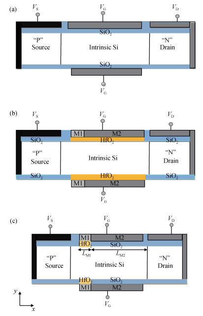
Fig. 1.
Device structure of (a) DLTFET, (b) DMG_DLTFET and (c) HD_DMG_DLTFET.
SEMICONDUCTOR DEVICES
Corresponding author: Sunny Anand,Email:sunnyanand.ec.13@nitj.ac.in
Abstract: In this paper, charge-plasma-based tunnel FET is proposed by employing dual material gate with hetero gate dielectric technique and it is named hetero-dielectric dual material gate doping-less TFET(HD_DMG_DLTFET). It is compared with conventional doping-less TFET(DLTFET) and dual material gate doping-less TFET(DMG_DLTFET) on the basis of analog and RF performance. The HD_DMG_DLTFET provides better ON state current(ION=94 μA/μm), ION/IOFF(≈ 1:36×1013), point(≈ 3 mV/dec) and average subthreshold slope(AV-SS=40.40 mV/dec). The proposed device offers low total gate capacitance(Cgg)along with higher drive current. However, with a better transconductance(gm) and cut-off frequency(fT), the HD_DMG_DLTFET can be a good candidate for RF circuitry. The early voltage(VEA) and output conductance(gd) are also moderate for the proposed device with comparison to other devices and therefore can be a candidate for analog devices. From all these simulation results and their study, it is observed that HD_DMG_DLTFET has improved analog/RF performance compared to DLTFET and DMG_DLTFET.
Key words: hetero-gate dielectric material, dual material gate, doping-less TFET, average subthreshold slope, analog FOM
| [1] |
?Young K K. Short-channel effect in fully-depleted SOI MOSFETs. IEEE Trans Electron Devices, 1989, 36(2):399 doi: 10.1109/16.19942
|
| [2] |
Colinge J P, Lee C W, Afzalian A, et al. Nanowire transistors without junctions. Nat Nanotechnol, 2010, 5(3):225 doi: 10.1038/nnano.2010.15
|
| [3] |
Koswatta S O, Lundstrom M S, Nikonov D E. Performance comparison between P-I-N tunneling transistors and conventional MOSFETs. IEEE Trans Electron Devices, 2009, 56(3):456 doi: 10.1109/TED.2008.2011934
|
| [4] |
Bernstein K, Cavin R K, Porod W, et al. Device and architectures outlook for beyond CMOS switches. Proc IEEE, 2010, 98:2169 doi: 10.1109/JPROC.2010.2066530
|
| [5] |
Boucart K, Ionescu A M. Double gate tunnel FET high-k gate dielectric. IEEE Trans Electron Devices, 2007, 54(7):1725 doi: 10.1109/TED.2007.899389
|
| [6] |
Bal P, Akram M W, Mondal P, et al. Performance estimation of sub-30 nm junctionless tunnel FET (JLTFET). J Comput Electron, 2013, 12:782 doi: 10.1007/s10825-013-0483-6
|
| [7] |
Cui N, Liang R, Xu J. Heteromaterial gate tunnel field effect transistor with lateral energy band profile modulation. Appl Phys Lett, 2011, 98(14):142105 doi: 10.1063/1.3574363
|
| [8] |
Boucart K, Ionescu A M. Length scaling of the double gate tunnel FET with a high-k gate dielectric. Solid-State Electron, 2007, 51(11):1500 http://cn.bing.com/academic/profile?id=abeb152da58cc5a01e71fb93f2fd0c52&encoded=0&v=paper_preview&mkt=zh-cn
|
| [9] |
Narang R, Gupta S M, Gupta R S, et al. Effect of temperature and gate stack on the linearity and analog performance of double gate tunnel FET. Berlin Heidelberg:Springer, 2011, 197:466 http://cn.bing.com/academic/profile?id=4630af11ca88b7756c2d4b3a54e7bb04&encoded=0&v=paper_preview&mkt=zh-cn
|
| [10] |
Singh G, Amin S I, Anand S, et al. Design of Si0.5Ge0.5 based tunnel field effect transistor and its performance evaluation. Superlattices Microstruct, 2016, 92:143 doi: 10.1016/j.spmi.2016.02.027
|
| [11] |
Lee M J, Choi W Y. Effects of device geometry on hetero-gatedielectric tunneling field-effect transistors. IEEE Electron Device Lett, 2012, 33(10):1459 doi: 10.1109/LED.2012.2206790
|
| [12] |
Wei L, Ou H, Kuo J M, et al. Dual-material gate (DMG) field effect transistor. IEEE Trans Electron Devices, 1999, 46(5):865 doi: 10.1109/16.760391
|
| [13] |
Saurabh S, Kumar M J. Novel attributes of a dual material gate nanoscale tunnel field-effect transistor. IEEE Trans Electron Devices, 2011, 58(2):404 doi: 10.1109/TED.2010.2093142
|
| [14] |
Damrongplasit N, Shin C, Kim S H, et al. Study of random dopant fluctuation effects in germanium-source tunnel FETs. IEEE Trans Electron Devices, 2011, 58(10):3541 doi: 10.1109/TED.2011.2161990
|
| [15] |
Kumar M J. Doping-less tunnel field effect transistor:design and investigation. IEEE Trans Electron Devices, 2013, 60(10):3285 doi: 10.1109/TED.2013.2276888
|
| [16] |
Rajasekharan B, Hueting R J E, Salm C, et al. Fabrication and characterization of the charge-plasma diode. IEEE Electron Device Lett, 2010, 31(6):528 doi: 10.1109/LED.2010.2045731
|
| [17] |
Hueting R J E, Rajasekharan B, Salm C, et al. The charge plasma p-n diode. IEEE Electron Device Lett, 2008, 29(12):1367 doi: 10.1109/LED.2008.2006864
|
| [18] |
Anand S, Amin S I, Sarin R K. Performance analysis of charge plasma based dual electrode tunnel FET. J Semicond, 2016, 37(5):054003 doi: 10.1088/1674-4926/37/5/054003
|
| [19] |
Anand S, Amin S I, Sarin R K. Analog performance investigation of dual electrode based doping-less tunnel FET. J Comput Electron, 2016, 15(1):103 http://cn.bing.com/academic/profile?id=9b961f8250fa301cbe698cb2c8ab5606&encoded=0&v=paper_preview&mkt=zh-cn
|
| [20] |
Chakraborty S, Mallik A. Subthreshold performance of dualmaterial gate CMOS devices and circuits for ultralow power analog/mixed-signal applications. IEEE Trans Electron Devices, 2008, 55(3):827 doi: 10.1109/TED.2007.914842
|
| [21] |
Ram M S, Abdi D B. Single grain boundary dopingless PNPN tunnel FET on recrystallized polysilicon:proposal and theoretical analysis. IEEE J Electron Devices Soc, 2015, 3(3):291 doi: 10.1109/JEDS.2015.2392618
|
| [22] |
Amin S I, Sarin R K. Charge-plasma based dual-material and gate-stacked architecture of junctionless transistor for enhanced analog performance. Superlattices Microstruct, 2015, 88:582 doi: 10.1016/j.spmi.2015.10.017
|
| [23] |
ATLAS device simulation software. Silvaco Int., Santa Clara, CA, USA, 2012
|
| [24] |
Rahi S B, Ghosh B, Bishnoi B. Temperature effect on hetero structure junctionless tunnel FET. J Semicond, 2015, 36(3):034002 doi: 10.1088/1674-4926/36/3/034002
|
| [25] |
Huang J H, Liu Z H, Jeng M C, et al. A physical model for MOSFET output resistance. International Electron Devices Meeting, 1992, 13:569 http://cn.bing.com/academic/profile?id=cb9b3981e9f9946aa8603e402034f0bc&encoded=0&v=paper_preview&mkt=zh-cn
|
| [26] |
Anand S, Sarin R K. An analysis on ambipolar reduction techniques for charge plasma based tunnel FETs. J Nanoelectron Optoelectron, 2016, 11:543 doi: 10.1166/jno.2016.1922
|
| [27] |
Singh S, Kondekar P N, Pal P. Transient performance estimation of charge plasma based negative capacitance junctionless tunnel FET. J Semicond, 2016, 37(2):024003 doi: 10.1088/1674-4926/37/2/024003
|
| [28] |
Sivasankaran K, Mallick P S. Impact of parameter fluctuations on RF stability performance of DG tunnel FET. J Semicond, 2015, 36(8):084001 doi: 10.1088/1674-4926/36/8/084001
|
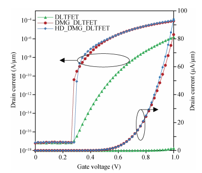

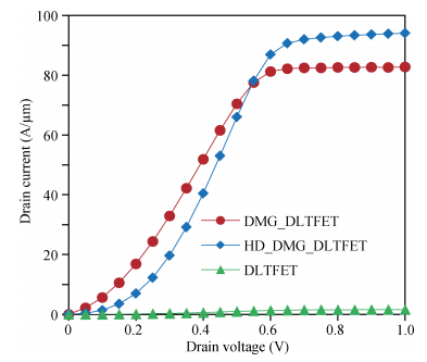
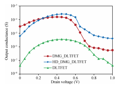
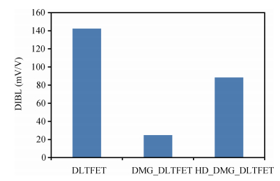
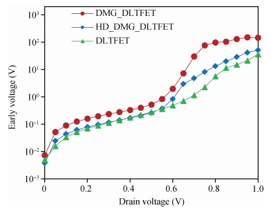
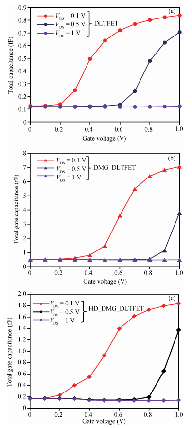
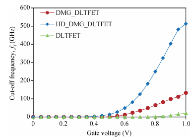
Table 1. Parameters used for DLTFET, DMG_DLTFET and HD_DMG_DLTFET.
 |
Table 2. Device characteristics of DLTFET, DMG_DLTFET and HD_DMG_DLTFET.
 |
| [1] |
?Young K K. Short-channel effect in fully-depleted SOI MOSFETs. IEEE Trans Electron Devices, 1989, 36(2):399 doi: 10.1109/16.19942
|
| [2] |
Colinge J P, Lee C W, Afzalian A, et al. Nanowire transistors without junctions. Nat Nanotechnol, 2010, 5(3):225 doi: 10.1038/nnano.2010.15
|
| [3] |
Koswatta S O, Lundstrom M S, Nikonov D E. Performance comparison between P-I-N tunneling transistors and conventional MOSFETs. IEEE Trans Electron Devices, 2009, 56(3):456 doi: 10.1109/TED.2008.2011934
|
| [4] |
Bernstein K, Cavin R K, Porod W, et al. Device and architectures outlook for beyond CMOS switches. Proc IEEE, 2010, 98:2169 doi: 10.1109/JPROC.2010.2066530
|
| [5] |
Boucart K, Ionescu A M. Double gate tunnel FET high-k gate dielectric. IEEE Trans Electron Devices, 2007, 54(7):1725 doi: 10.1109/TED.2007.899389
|
| [6] |
Bal P, Akram M W, Mondal P, et al. Performance estimation of sub-30 nm junctionless tunnel FET (JLTFET). J Comput Electron, 2013, 12:782 doi: 10.1007/s10825-013-0483-6
|
| [7] |
Cui N, Liang R, Xu J. Heteromaterial gate tunnel field effect transistor with lateral energy band profile modulation. Appl Phys Lett, 2011, 98(14):142105 doi: 10.1063/1.3574363
|
| [8] |
Boucart K, Ionescu A M. Length scaling of the double gate tunnel FET with a high-k gate dielectric. Solid-State Electron, 2007, 51(11):1500 http://cn.bing.com/academic/profile?id=abeb152da58cc5a01e71fb93f2fd0c52&encoded=0&v=paper_preview&mkt=zh-cn
|
| [9] |
Narang R, Gupta S M, Gupta R S, et al. Effect of temperature and gate stack on the linearity and analog performance of double gate tunnel FET. Berlin Heidelberg:Springer, 2011, 197:466 http://cn.bing.com/academic/profile?id=4630af11ca88b7756c2d4b3a54e7bb04&encoded=0&v=paper_preview&mkt=zh-cn
|
| [10] |
Singh G, Amin S I, Anand S, et al. Design of Si0.5Ge0.5 based tunnel field effect transistor and its performance evaluation. Superlattices Microstruct, 2016, 92:143 doi: 10.1016/j.spmi.2016.02.027
|
| [11] |
Lee M J, Choi W Y. Effects of device geometry on hetero-gatedielectric tunneling field-effect transistors. IEEE Electron Device Lett, 2012, 33(10):1459 doi: 10.1109/LED.2012.2206790
|
| [12] |
Wei L, Ou H, Kuo J M, et al. Dual-material gate (DMG) field effect transistor. IEEE Trans Electron Devices, 1999, 46(5):865 doi: 10.1109/16.760391
|
| [13] |
Saurabh S, Kumar M J. Novel attributes of a dual material gate nanoscale tunnel field-effect transistor. IEEE Trans Electron Devices, 2011, 58(2):404 doi: 10.1109/TED.2010.2093142
|
| [14] |
Damrongplasit N, Shin C, Kim S H, et al. Study of random dopant fluctuation effects in germanium-source tunnel FETs. IEEE Trans Electron Devices, 2011, 58(10):3541 doi: 10.1109/TED.2011.2161990
|
| [15] |
Kumar M J. Doping-less tunnel field effect transistor:design and investigation. IEEE Trans Electron Devices, 2013, 60(10):3285 doi: 10.1109/TED.2013.2276888
|
| [16] |
Rajasekharan B, Hueting R J E, Salm C, et al. Fabrication and characterization of the charge-plasma diode. IEEE Electron Device Lett, 2010, 31(6):528 doi: 10.1109/LED.2010.2045731
|
| [17] |
Hueting R J E, Rajasekharan B, Salm C, et al. The charge plasma p-n diode. IEEE Electron Device Lett, 2008, 29(12):1367 doi: 10.1109/LED.2008.2006864
|
| [18] |
Anand S, Amin S I, Sarin R K. Performance analysis of charge plasma based dual electrode tunnel FET. J Semicond, 2016, 37(5):054003 doi: 10.1088/1674-4926/37/5/054003
|
| [19] |
Anand S, Amin S I, Sarin R K. Analog performance investigation of dual electrode based doping-less tunnel FET. J Comput Electron, 2016, 15(1):103 http://cn.bing.com/academic/profile?id=9b961f8250fa301cbe698cb2c8ab5606&encoded=0&v=paper_preview&mkt=zh-cn
|
| [20] |
Chakraborty S, Mallik A. Subthreshold performance of dualmaterial gate CMOS devices and circuits for ultralow power analog/mixed-signal applications. IEEE Trans Electron Devices, 2008, 55(3):827 doi: 10.1109/TED.2007.914842
|
| [21] |
Ram M S, Abdi D B. Single grain boundary dopingless PNPN tunnel FET on recrystallized polysilicon:proposal and theoretical analysis. IEEE J Electron Devices Soc, 2015, 3(3):291 doi: 10.1109/JEDS.2015.2392618
|
| [22] |
Amin S I, Sarin R K. Charge-plasma based dual-material and gate-stacked architecture of junctionless transistor for enhanced analog performance. Superlattices Microstruct, 2015, 88:582 doi: 10.1016/j.spmi.2015.10.017
|
| [23] |
ATLAS device simulation software. Silvaco Int., Santa Clara, CA, USA, 2012
|
| [24] |
Rahi S B, Ghosh B, Bishnoi B. Temperature effect on hetero structure junctionless tunnel FET. J Semicond, 2015, 36(3):034002 doi: 10.1088/1674-4926/36/3/034002
|
| [25] |
Huang J H, Liu Z H, Jeng M C, et al. A physical model for MOSFET output resistance. International Electron Devices Meeting, 1992, 13:569 http://cn.bing.com/academic/profile?id=cb9b3981e9f9946aa8603e402034f0bc&encoded=0&v=paper_preview&mkt=zh-cn
|
| [26] |
Anand S, Sarin R K. An analysis on ambipolar reduction techniques for charge plasma based tunnel FETs. J Nanoelectron Optoelectron, 2016, 11:543 doi: 10.1166/jno.2016.1922
|
| [27] |
Singh S, Kondekar P N, Pal P. Transient performance estimation of charge plasma based negative capacitance junctionless tunnel FET. J Semicond, 2016, 37(2):024003 doi: 10.1088/1674-4926/37/2/024003
|
| [28] |
Sivasankaran K, Mallick P S. Impact of parameter fluctuations on RF stability performance of DG tunnel FET. J Semicond, 2015, 36(8):084001 doi: 10.1088/1674-4926/36/8/084001
|


Article views: 3741 Times PDF downloads: 32 Times Cited by: 0 Times
Received: 16 May 2016 Revised: 02 August 2016 Online: Published: 01 February 2017
| Citation: |
Sunny Anand, R.K. Sarin. Dual material gate doping-less tunnel FET with hetero gate dielectric for enhancement of analog/RF performance[J]. Journal of Semiconductors, 2017, 38(2): 024001. doi: 10.1088/1674-4926/38/2/024001
****
S Anand, R K Sarin. Dual material gate doping-less tunnel FET with hetero gate dielectric for enhancement of analog/RF performance[J]. J. Semicond., 2017, 38(2): 024001. doi:? 10.1088/1674-4926/38/2/024001.

|
the Special Foundation of President of China Academy of Engineering Physics 2014-1-100
Project supported by the Science and Technology Development Foundation of China Academy of Engineering Physics(No.2014A05011) and the Special Foundation of President of China Academy of Engineering Physics(No.2014-1-100).
Project supported by the Science and Technology Development Foundation of China Academy of Engineering Physics 2014A05011
| [1] |
?Young K K. Short-channel effect in fully-depleted SOI MOSFETs. IEEE Trans Electron Devices, 1989, 36(2):399 doi: 10.1109/16.19942
|
| [2] |
Colinge J P, Lee C W, Afzalian A, et al. Nanowire transistors without junctions. Nat Nanotechnol, 2010, 5(3):225 doi: 10.1038/nnano.2010.15
|
| [3] |
Koswatta S O, Lundstrom M S, Nikonov D E. Performance comparison between P-I-N tunneling transistors and conventional MOSFETs. IEEE Trans Electron Devices, 2009, 56(3):456 doi: 10.1109/TED.2008.2011934
|
| [4] |
Bernstein K, Cavin R K, Porod W, et al. Device and architectures outlook for beyond CMOS switches. Proc IEEE, 2010, 98:2169 doi: 10.1109/JPROC.2010.2066530
|
| [5] |
Boucart K, Ionescu A M. Double gate tunnel FET high-k gate dielectric. IEEE Trans Electron Devices, 2007, 54(7):1725 doi: 10.1109/TED.2007.899389
|
| [6] |
Bal P, Akram M W, Mondal P, et al. Performance estimation of sub-30 nm junctionless tunnel FET (JLTFET). J Comput Electron, 2013, 12:782 doi: 10.1007/s10825-013-0483-6
|
| [7] |
Cui N, Liang R, Xu J. Heteromaterial gate tunnel field effect transistor with lateral energy band profile modulation. Appl Phys Lett, 2011, 98(14):142105 doi: 10.1063/1.3574363
|
| [8] |
Boucart K, Ionescu A M. Length scaling of the double gate tunnel FET with a high-k gate dielectric. Solid-State Electron, 2007, 51(11):1500 http://cn.bing.com/academic/profile?id=abeb152da58cc5a01e71fb93f2fd0c52&encoded=0&v=paper_preview&mkt=zh-cn
|
| [9] |
Narang R, Gupta S M, Gupta R S, et al. Effect of temperature and gate stack on the linearity and analog performance of double gate tunnel FET. Berlin Heidelberg:Springer, 2011, 197:466 http://cn.bing.com/academic/profile?id=4630af11ca88b7756c2d4b3a54e7bb04&encoded=0&v=paper_preview&mkt=zh-cn
|
| [10] |
Singh G, Amin S I, Anand S, et al. Design of Si0.5Ge0.5 based tunnel field effect transistor and its performance evaluation. Superlattices Microstruct, 2016, 92:143 doi: 10.1016/j.spmi.2016.02.027
|
| [11] |
Lee M J, Choi W Y. Effects of device geometry on hetero-gatedielectric tunneling field-effect transistors. IEEE Electron Device Lett, 2012, 33(10):1459 doi: 10.1109/LED.2012.2206790
|
| [12] |
Wei L, Ou H, Kuo J M, et al. Dual-material gate (DMG) field effect transistor. IEEE Trans Electron Devices, 1999, 46(5):865 doi: 10.1109/16.760391
|
| [13] |
Saurabh S, Kumar M J. Novel attributes of a dual material gate nanoscale tunnel field-effect transistor. IEEE Trans Electron Devices, 2011, 58(2):404 doi: 10.1109/TED.2010.2093142
|
| [14] |
Damrongplasit N, Shin C, Kim S H, et al. Study of random dopant fluctuation effects in germanium-source tunnel FETs. IEEE Trans Electron Devices, 2011, 58(10):3541 doi: 10.1109/TED.2011.2161990
|
| [15] |
Kumar M J. Doping-less tunnel field effect transistor:design and investigation. IEEE Trans Electron Devices, 2013, 60(10):3285 doi: 10.1109/TED.2013.2276888
|
| [16] |
Rajasekharan B, Hueting R J E, Salm C, et al. Fabrication and characterization of the charge-plasma diode. IEEE Electron Device Lett, 2010, 31(6):528 doi: 10.1109/LED.2010.2045731
|
| [17] |
Hueting R J E, Rajasekharan B, Salm C, et al. The charge plasma p-n diode. IEEE Electron Device Lett, 2008, 29(12):1367 doi: 10.1109/LED.2008.2006864
|
| [18] |
Anand S, Amin S I, Sarin R K. Performance analysis of charge plasma based dual electrode tunnel FET. J Semicond, 2016, 37(5):054003 doi: 10.1088/1674-4926/37/5/054003
|
| [19] |
Anand S, Amin S I, Sarin R K. Analog performance investigation of dual electrode based doping-less tunnel FET. J Comput Electron, 2016, 15(1):103 http://cn.bing.com/academic/profile?id=9b961f8250fa301cbe698cb2c8ab5606&encoded=0&v=paper_preview&mkt=zh-cn
|
| [20] |
Chakraborty S, Mallik A. Subthreshold performance of dualmaterial gate CMOS devices and circuits for ultralow power analog/mixed-signal applications. IEEE Trans Electron Devices, 2008, 55(3):827 doi: 10.1109/TED.2007.914842
|
| [21] |
Ram M S, Abdi D B. Single grain boundary dopingless PNPN tunnel FET on recrystallized polysilicon:proposal and theoretical analysis. IEEE J Electron Devices Soc, 2015, 3(3):291 doi: 10.1109/JEDS.2015.2392618
|
| [22] |
Amin S I, Sarin R K. Charge-plasma based dual-material and gate-stacked architecture of junctionless transistor for enhanced analog performance. Superlattices Microstruct, 2015, 88:582 doi: 10.1016/j.spmi.2015.10.017
|
| [23] |
ATLAS device simulation software. Silvaco Int., Santa Clara, CA, USA, 2012
|
| [24] |
Rahi S B, Ghosh B, Bishnoi B. Temperature effect on hetero structure junctionless tunnel FET. J Semicond, 2015, 36(3):034002 doi: 10.1088/1674-4926/36/3/034002
|
| [25] |
Huang J H, Liu Z H, Jeng M C, et al. A physical model for MOSFET output resistance. International Electron Devices Meeting, 1992, 13:569 http://cn.bing.com/academic/profile?id=cb9b3981e9f9946aa8603e402034f0bc&encoded=0&v=paper_preview&mkt=zh-cn
|
| [26] |
Anand S, Sarin R K. An analysis on ambipolar reduction techniques for charge plasma based tunnel FETs. J Nanoelectron Optoelectron, 2016, 11:543 doi: 10.1166/jno.2016.1922
|
| [27] |
Singh S, Kondekar P N, Pal P. Transient performance estimation of charge plasma based negative capacitance junctionless tunnel FET. J Semicond, 2016, 37(2):024003 doi: 10.1088/1674-4926/37/2/024003
|
| [28] |
Sivasankaran K, Mallick P S. Impact of parameter fluctuations on RF stability performance of DG tunnel FET. J Semicond, 2015, 36(8):084001 doi: 10.1088/1674-4926/36/8/084001
|

 WeChat ID
Journal of Semiconductors © 2017 All Rights Reserved 京ICP備05085259號(hào)-2
 DownLoad:

