


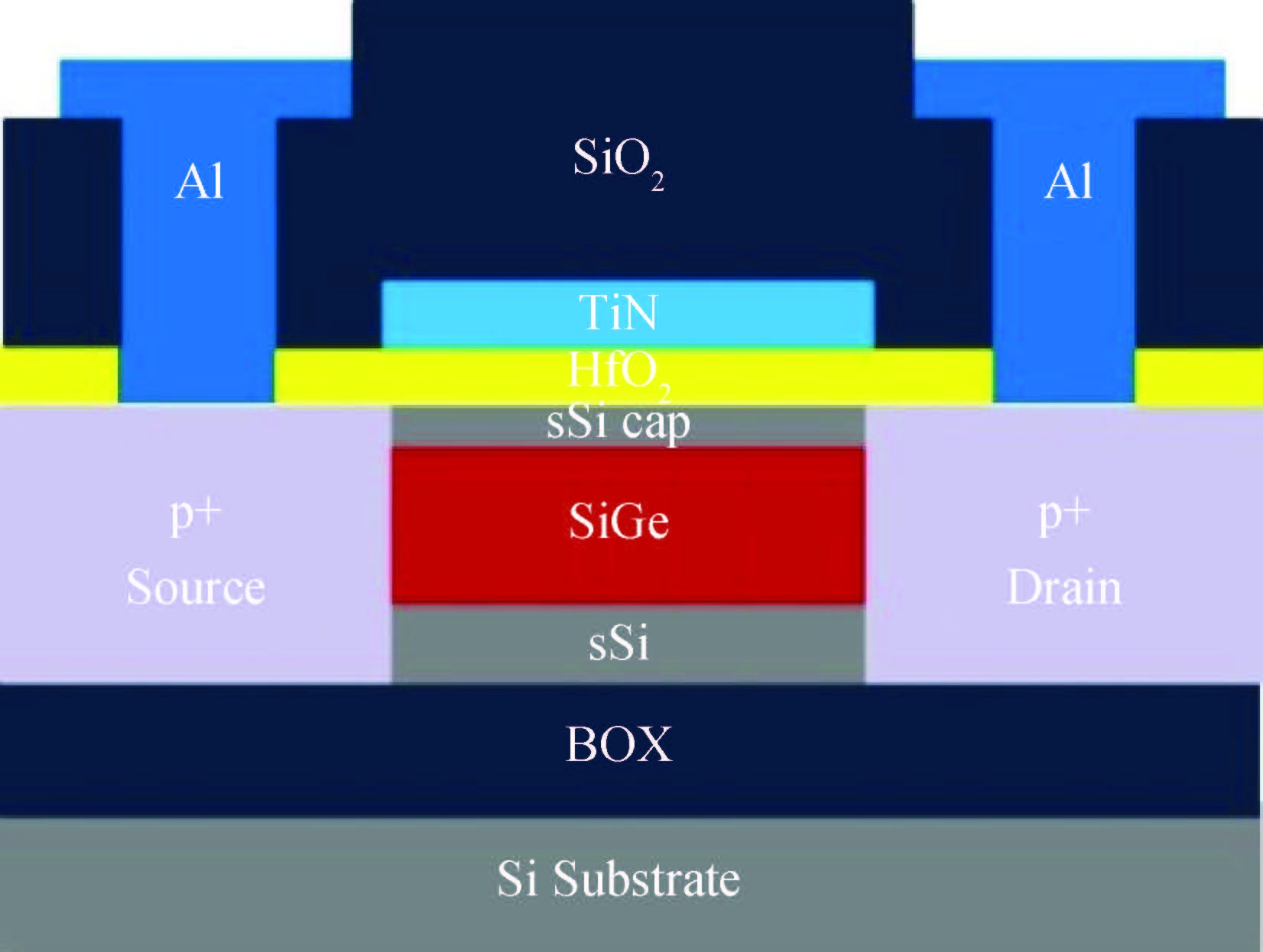
Fig. 1.
(Color online) Schematic view of sSi/Si0.5Ge0.5/sSOI QW p-MOSFET's cross-section.
SEMICONDUCTOR DEVICES
Jiao Wen1, 2, Qiang Liu1, 2, Chang Liu2, Yize Wang2, Bo Zhang2, Zhongying Xue2, Zengfeng Di2, Wenjie Yu2, and Qingtai Zhao3
Corresponding author: Wenjie Yu, casan@mail.sim.ac.cn
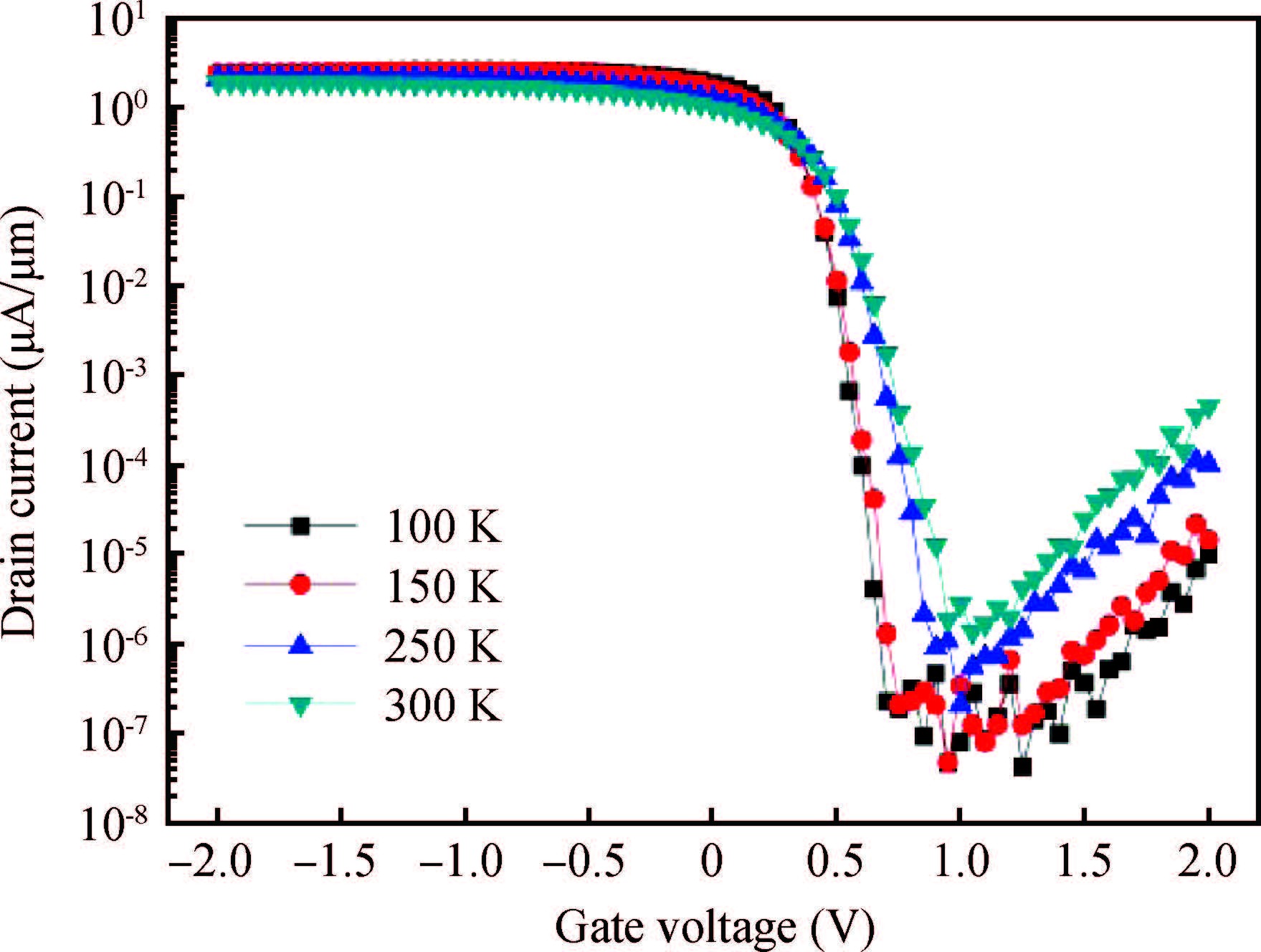
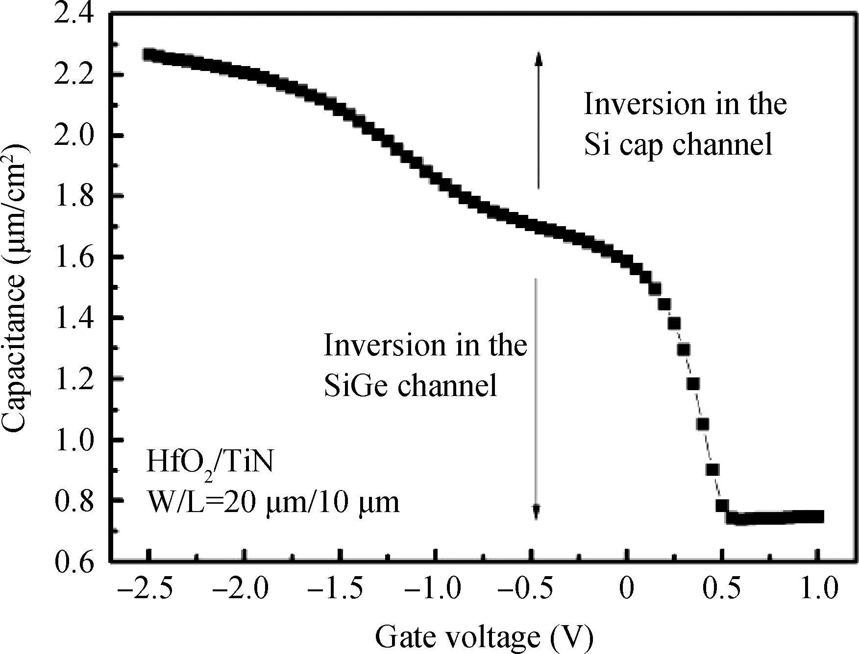
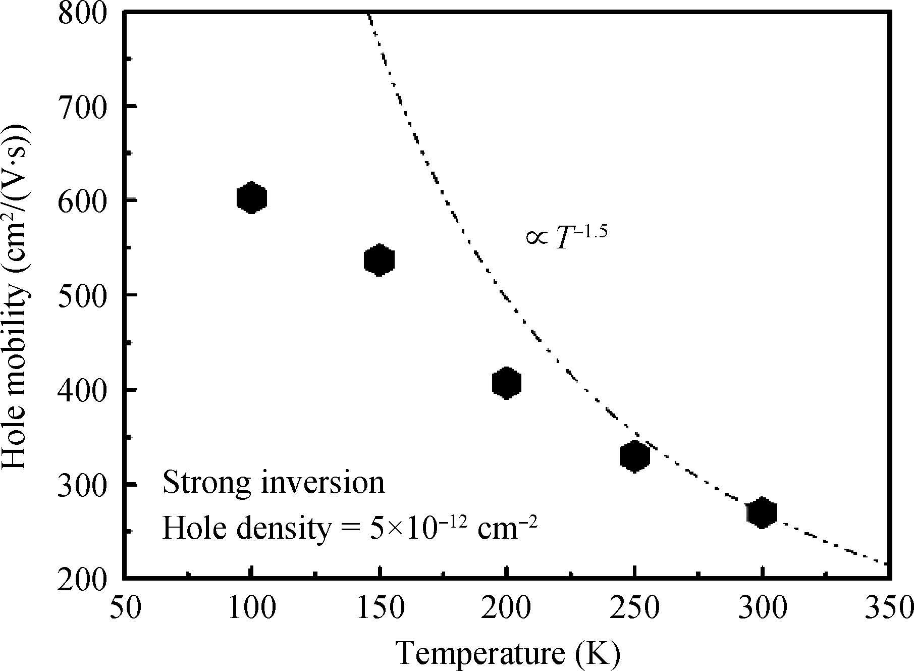
Abstract: sSi/Si0.5Ge0.5/sSOI quantum-well (QW) p-MOSFETs with HfO2/TiN gate stack were fabricated and characterized. According to the low temperature experimental results, carrier mobility of the strained Si0.5Ge0.5 QW p-MOSFET was mainly governed by phonon scattering from 300 to 150 K and Coulomb scattering below 150 K, respectively. Coulomb scattering was intensified by the accumulated inversion charges in the Si cap layer of this Si/SiGe heterostructure, which led to a degradation of carrier mobility in the SiGe channel, especially at low temperature.
Key words: SiGe, quantum-well, hole mobility, Coulomb scattering
| [1] |
Hill R J W, Moran D A J, Li X, et al. Enhancement-mode GaAs MOSFETs with an In0.3Ga0.7As channel, a mobility of over 5000 cm2/(V· s), and transconductance of over 475μS/μm. IEEE Electron Device Lett, 2007, 28(12): 1080 doi: 10.1109/LED.2007.910009
|
| [2] |
Lee M L, Fitzgerald E A, Bulsara M T, et al. Strained Si, SiGe, and Ge channels for high-mobility metal-oxide-semiconductor field-effect transistors. J Appl Phys, 2005, 97(1): 011101 doi: 10.1063/1.1819976
|
| [3] |
Takagi S, Tezuka T, Irisawa T, et al. Device structures and carrier transport properties of advanced CMOS using high mobility channels. Solid-State Electron, 2007, 51(4): 526 doi: 10.1016/j.sse.2007.02.017
|
| [4] |
Cui W, Tang Z H, Tan K Z, et al. A strained Si-channel NMOSFET with low field mobility enhancement of about 140% using a SiGe virtual substrate. Journal of Semiconductors, 2012, 33(9): 094005 doi: 10.1088/1674-4926/33/9/094005
|
| [5] |
Chaudhry A, Roy J N, Garima J. Nanoscale strained-Si MOSFET physics and modeling approaches: a review. Journal of Semiconductors, 2010, 31(10): 104001 doi: 10.1088/1674-4926/31/10/104001
|
| [6] |
Von Haartman M, Malm B G, Ostling M. Comprehensive study on low-frequency noise and mobility in Si and SiGe PMOSFETS with high-k gate dielectrics and TiN gate. IEEE Trans Electron Devices, 2006, 53(4): 836 doi: 10.1109/TED.2006.870276
|
| [7] |
Gomez L, Hashemi P, Hoyt J L. Enhanced hole transport in short-channel strained-SiGe p-MOSFETs. IEEE Trans Electron Devices, 2009, 56(11): 2644 doi: 10.1109/TED.2009.2031043
|
| [8] |
Loo R, Sorada H, Inoue A, et al. Selective epitaxial Si/SiGe growth for VT shift adjustment in high-κ pMOS devices. Semicond Sci Technol, 2007, 22(1): 110 doi: 10.1088/0268-1242/22/1/S26
|
| [9] |
Fischetti M, Laux S. Band structure, deformation potentials, and carrier mobility in strained Si, Ge, and SiGe alloys. J Appl Phys, 1996, 80(4): 2234 doi: 10.1063/1.363052
|
| [10] |
Cassé M, Hutin L, Le Royer C, et al. Experimental investigation of hole transport in strained Si1-xGex/SOI pMOSFETs-Part I: scattering mechanisms in long-channel devices. IEEE Trans Electron Devices, 2012, 59(2): 316 doi: 10.1109/TED.2011.2175735
|
| [11] |
Yu W, Wu W R, Zhang B, et al. Experimental investigation on alloy scattering in sSi/Si0.5Ge0.5/sSOI quantum-well p-MOSFET. IEEE Trans Electron Devices, 2014, 61(4): 950 doi: 10.1109/TED.2014.2304723
|
| [12] |
Chattopadhyay S, Kwa K S K, Olsen S, et al. C-V characterization of strained Si/SiGe multiple heterojunction capacitors as a tool for heterojunction MOSFET channel design. Semicond Sci Technol, 2003, 18(8): 738 doi: 10.1088/0268-1242/18/8/304
|
| [13] |
Garone P M, Venkataraman V, Sturm J C. Hole mobility enhancement in MOS-gated GexSi1-x/Si heterostructure inversion layers. IEEE Electron Device Lett, 1992, 13(1): 56 doi: 10.1109/55.144950
|
| [14] |
Weber O, Damlencourt J F, Andrieu F, et al. Fabrication and mobility characteristics of SiGe surface channel p-MOSFETs with a HfO2/TiN gate stack. IEEE Trans Electron Devices, 2006, 53(3): 449 doi: 10.1109/TED.2005.863536
|
| [15] |
Song Y J, Lim J W, Kim S H, et al. Effects of Si-cap layer thinning and Ge segregation on the characteristics of Si/SiGe/Si heterostructure p-MOSFETs. Solid-State Electron, 2002, 46: 1983 doi: 10.1016/S0038-1101(02)00139-9
|
| [16] |
Takagi S, Toriumi A, Iwase M, et al. On the universality of inversion layer mobility in Si MOSFETs: Part ??-effect of surface orientation. IEEE Trans Electron Devices, 1994, 41(12): 2363 doi: 10.1109/16.337450
|
| [17] |
Takagi S, Toriumi A, Iwase M, et al. On the universality of inversion layer mobility in Si MOSFET's: Part I-effects of substrate impurity concentration. IEEE Trans Electron Devices, 1994, 41(12): 2357 doi: 10.1109/16.337449
|
| [18] |
Kearney M J, Horrell A I. The effect of alloy scattering on the mobility of holes in a Si1-xGex quantum well. Semicond Sci Technol, 1998, 13(2): 174 doi: 10.1088/0268-1242/13/2/003
|
| [19] |
H?ck G, Kohn E, Rosenblad C, et al. High hole mobility in Si0.17Ge0.83 channel metal-oxide-semiconductor field-effect transistors grown by plasma-enhanced chemical vapor deposition. Appl Phys Lett, 2000, 76(26): 3920 doi: 10.1063/1.126821
|
| [20] |
Andrieu F, Ernst T, Romanjek K, et al. SiGe channel p-MOSFETs scaling-down. Proceedings of European Solid-State Device Research Conference, 2003: 267 http://cn.bing.com/academic/profile?id=1595437296&encoded=0&v=paper_preview&mkt=zh-cn
|


Article views: 3416 Times PDF downloads: 23 Times Cited by: 0 Times
Received: 16 February 2016 Revised: 21 March 2016 Online: Published: 01 September 2016
| Citation: |
Jiao Wen, Qiang Liu, Chang Liu, Yize Wang, Bo Zhang, Zhongying Xue, Zengfeng Di, Wenjie Yu, Qingtai Zhao. Investigation of Coulomb scattering on sSi/Si0.5Ge0.5/sSOI quantum-well p-MOSFETs[J]. Journal of Semiconductors, 2016, 37(9): 094002. doi: 10.1088/1674-4926/37/9/094002
****
J Wen, Q Liu, C Liu, Y Z Wang, B Zhang, Z Y Xue, Z F Di, W J Yu, Q T Zhao. Investigation of Coulomb scattering on sSi/Si0.5Ge0.5/sSOI quantum-well p-MOSFETs[J]. J. Semicond., 2016, 37(9): 094002. doi: 10.1088/1674-4926/37/9/094002.

|
Project supported by the National Natural Science Foundation of China (Nos. 61306126, 61306127, 61106015) and the CAS International Collaboration and Innovation Program on High Mobility Materials Engineering
the CAS International Collaboration and Innovation Program on High Mobility Materials Engineering
Project supported by the National Natural Science Foundation of China Nos. 61306126, 61306127, 61106015
| [1] |
Hill R J W, Moran D A J, Li X, et al. Enhancement-mode GaAs MOSFETs with an In0.3Ga0.7As channel, a mobility of over 5000 cm2/(V· s), and transconductance of over 475μS/μm. IEEE Electron Device Lett, 2007, 28(12): 1080 doi: 10.1109/LED.2007.910009
|
| [2] |
Lee M L, Fitzgerald E A, Bulsara M T, et al. Strained Si, SiGe, and Ge channels for high-mobility metal-oxide-semiconductor field-effect transistors. J Appl Phys, 2005, 97(1): 011101 doi: 10.1063/1.1819976
|
| [3] |
Takagi S, Tezuka T, Irisawa T, et al. Device structures and carrier transport properties of advanced CMOS using high mobility channels. Solid-State Electron, 2007, 51(4): 526 doi: 10.1016/j.sse.2007.02.017
|
| [4] |
Cui W, Tang Z H, Tan K Z, et al. A strained Si-channel NMOSFET with low field mobility enhancement of about 140% using a SiGe virtual substrate. Journal of Semiconductors, 2012, 33(9): 094005 doi: 10.1088/1674-4926/33/9/094005
|
| [5] |
Chaudhry A, Roy J N, Garima J. Nanoscale strained-Si MOSFET physics and modeling approaches: a review. Journal of Semiconductors, 2010, 31(10): 104001 doi: 10.1088/1674-4926/31/10/104001
|
| [6] |
Von Haartman M, Malm B G, Ostling M. Comprehensive study on low-frequency noise and mobility in Si and SiGe PMOSFETS with high-k gate dielectrics and TiN gate. IEEE Trans Electron Devices, 2006, 53(4): 836 doi: 10.1109/TED.2006.870276
|
| [7] |
Gomez L, Hashemi P, Hoyt J L. Enhanced hole transport in short-channel strained-SiGe p-MOSFETs. IEEE Trans Electron Devices, 2009, 56(11): 2644 doi: 10.1109/TED.2009.2031043
|
| [8] |
Loo R, Sorada H, Inoue A, et al. Selective epitaxial Si/SiGe growth for VT shift adjustment in high-κ pMOS devices. Semicond Sci Technol, 2007, 22(1): 110 doi: 10.1088/0268-1242/22/1/S26
|
| [9] |
Fischetti M, Laux S. Band structure, deformation potentials, and carrier mobility in strained Si, Ge, and SiGe alloys. J Appl Phys, 1996, 80(4): 2234 doi: 10.1063/1.363052
|
| [10] |
Cassé M, Hutin L, Le Royer C, et al. Experimental investigation of hole transport in strained Si1-xGex/SOI pMOSFETs-Part I: scattering mechanisms in long-channel devices. IEEE Trans Electron Devices, 2012, 59(2): 316 doi: 10.1109/TED.2011.2175735
|
| [11] |
Yu W, Wu W R, Zhang B, et al. Experimental investigation on alloy scattering in sSi/Si0.5Ge0.5/sSOI quantum-well p-MOSFET. IEEE Trans Electron Devices, 2014, 61(4): 950 doi: 10.1109/TED.2014.2304723
|
| [12] |
Chattopadhyay S, Kwa K S K, Olsen S, et al. C-V characterization of strained Si/SiGe multiple heterojunction capacitors as a tool for heterojunction MOSFET channel design. Semicond Sci Technol, 2003, 18(8): 738 doi: 10.1088/0268-1242/18/8/304
|
| [13] |
Garone P M, Venkataraman V, Sturm J C. Hole mobility enhancement in MOS-gated GexSi1-x/Si heterostructure inversion layers. IEEE Electron Device Lett, 1992, 13(1): 56 doi: 10.1109/55.144950
|
| [14] |
Weber O, Damlencourt J F, Andrieu F, et al. Fabrication and mobility characteristics of SiGe surface channel p-MOSFETs with a HfO2/TiN gate stack. IEEE Trans Electron Devices, 2006, 53(3): 449 doi: 10.1109/TED.2005.863536
|
| [15] |
Song Y J, Lim J W, Kim S H, et al. Effects of Si-cap layer thinning and Ge segregation on the characteristics of Si/SiGe/Si heterostructure p-MOSFETs. Solid-State Electron, 2002, 46: 1983 doi: 10.1016/S0038-1101(02)00139-9
|
| [16] |
Takagi S, Toriumi A, Iwase M, et al. On the universality of inversion layer mobility in Si MOSFETs: Part ??-effect of surface orientation. IEEE Trans Electron Devices, 1994, 41(12): 2363 doi: 10.1109/16.337450
|
| [17] |
Takagi S, Toriumi A, Iwase M, et al. On the universality of inversion layer mobility in Si MOSFET's: Part I-effects of substrate impurity concentration. IEEE Trans Electron Devices, 1994, 41(12): 2357 doi: 10.1109/16.337449
|
| [18] |
Kearney M J, Horrell A I. The effect of alloy scattering on the mobility of holes in a Si1-xGex quantum well. Semicond Sci Technol, 1998, 13(2): 174 doi: 10.1088/0268-1242/13/2/003
|
| [19] |
H?ck G, Kohn E, Rosenblad C, et al. High hole mobility in Si0.17Ge0.83 channel metal-oxide-semiconductor field-effect transistors grown by plasma-enhanced chemical vapor deposition. Appl Phys Lett, 2000, 76(26): 3920 doi: 10.1063/1.126821
|
| [20] |
Andrieu F, Ernst T, Romanjek K, et al. SiGe channel p-MOSFETs scaling-down. Proceedings of European Solid-State Device Research Conference, 2003: 267 http://cn.bing.com/academic/profile?id=1595437296&encoded=0&v=paper_preview&mkt=zh-cn
|

 WeChat ID
Journal of Semiconductors © 2017 All Rights Reserved 京ICP備05085259號(hào)-2
 DownLoad:

