


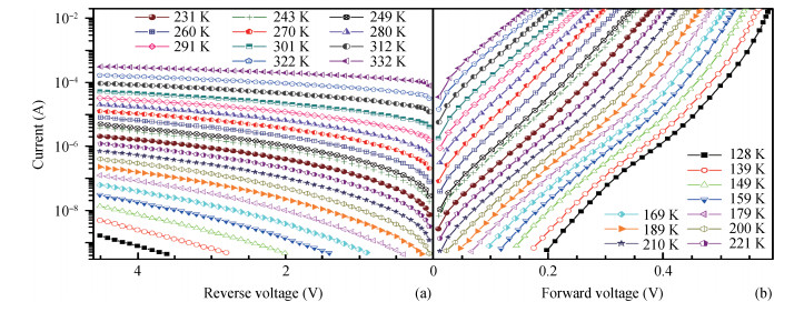
Fig. 1.
(Color online) (a) Reverse and (b) forward I–V characteristics of Mo/n–Si Schottky structures measured at 10 K intervals without USL. The lines are added to guide the eye.
SEMICONDUCTOR PHYSICS
O.Ya Olikh1, , K.V. Voitenko1, R.M. Burbelo1 and JaM. Olikh2
Corresponding author: O. Ya Olikh, Email:olikh@univ.kiev.ua
Abstract: The influence of ultrasonic loading on reverse current-voltage characteristics of Mo/n-n+-Si structures has been investigated. The research of leakage current variation has been carried out for various ultrasonic wave frequencies (4.1 and 8.4 MHz), intensities (up to 0.8 W/cm2) and loading temperatures (130-330 K). The observed reversible acoustically induced increase in reverse currents was as large as 60%. It has been found that dominant charge transfer mechanisms are the thermionic emission (at high temperature) and the phonon-assisted tunneling (at low temperature). The ultrasound loading affects both processes due to the decrease of Schottky barrier height and binding energy of the electron on the trap.
Key words: Schottky contact, leakage current, ultrasound influence
| [1] |
Savkina R K, Smirnov A B, Sizov F. The effect of high-frequency sonication on charge carrier transport in LPE and MBE HgCdTe layers. Semicond Sci Technol, 2007, 22(2): 97 doi: 10.1088/0268-1242/22/2/016
|
| [2] |
Kulakova L, Gorelov V, Lutetskiy A, et al. The rotation of the polarization plane of quantum-well heterolasers emission under the ultrasonic strain. Solid State Commun, 2012, 152(17): 1690 doi: 10.1016/j.ssc.2012.04.065
|
| [3] |
Ostrovskii I, Korotchenkov O, Olikh O, et al. Acoustically driven optical phenomena in bulk and low-dimensional semiconductors. J Opt A, 2001, 3(4): S82 https://www.researchgate.net/publication/230991018_Acoustically_driven_optical_phenomena_in_bulk_and_low-dimensional_semiconductors
|
| [4] |
Buyukkose S, Vratzov B, van der Veen J, et al. Ultrahighfrequency surface acoustic wave generation for acoustic charge transport in silicon. Appl Phys Lett, 2013, 102(1): 013112 doi: 10.1063/1.4774388
|
| [5] |
He J H, Gao J, Guo H Z. Correlated electron transport assisted by surface acoustic waves in micron-separated quasi-onedimensional channels. Appl Phys Lett, 2010, 97(12): 122107 doi: 10.1063/1.3491287
|
| [6] |
Ostapenko S S, L Jastrzebski, Sopori B. Change of minority carrier diffusion length in polycrystalline silicon by ultrasound treatment. Semicond Sci Technol, 1995, 10(11): 1494 doi: 10.1088/0268-1242/10/11/011
|
| [7] |
Ostapenko S. Defect passivation using ultrasound treatment: fundamentals and application. Appl Phys A: Mater Sci Process, 1999, 69(2): 225 doi: 10.1007/s003390050994
|
| [8] |
Sukach A, Teterkin V. Ultrasonic treatment-induced modification of the electrical properties of InAs p-n junctions. Tech Phys Lett, 2009, 35(6): 514 doi: 10.1134/S1063785009060108
|
| [9] |
Olikh O. Features of dynamic acoustically induced modification of photovoltaic parameters of silicon solar cells. Semiconductors, 2011, 45(6): 798 doi: 10.1134/S1063782611060170
|
| [10] |
Davletova A, Karazhanov S Z. A study of electrical properties of dislocation engineered Si processed by ultrasound. J Phys Chem Solids, 2009, 70(6): 989 doi: 10.1016/j.jpcs.2009.05.009
|
| [11] |
Davletova A, Karazhanov S Z. Open-circuit voltage decay transient in dislocation-engineered Si p-n junction. J Phys D: Appl Phys, 2008, 41(16): 165107 doi: 10.1088/0022-3727/41/16/165107
|
| [12] |
Melnik V, Olikh Y, Popov V, et al. Characteristics of silicon p-n junction formed by ion implantation with in situ ultrasound treatment. Mater Sci Eng B, 2005, 124/125: 327 doi: 10.1016/j.mseb.2005.08.039
|
| [13] |
Olikh O. Effect of ultrasonic loading on current in Mo/n-n+-Si with Schottky barriers. Semiconductors, 2013, 47(7): 987 doi: 10.1134/S106378261307018X
|
| [14] |
Olikh O. Reversible influence of ultrasound on γ-irradiated Mo/n-Si Schottky barrier structure. Ultrasonics, 2015, 56: 545 doi: 10.1016/j.ultras.2014.10.008
|
| [15] |
Zaveryukhina N, Zaveryukhina E, Vlasov S, et al. Acoustostimulated changes in the density of surface states and their energy spectrum in p-type silicon single crystals. Tech Phys Lett, 2008, 34(3): 241 doi: 10.1134/S106378500803019X
|
| [16] |
Mirsagatov S A, Sapaeva I B, Nazarov Z. Ultrasonic annealing of surface states in the heterojunction of a p-Si/n-CdS/n+-CdS injection photodiode. Inorg Mater, 2015, 51(1): 1 doi: 10.1134/S0020168515010148
|
| [17] |
Wosinski T, Makosa A, Witczak Z. Transformation of native defects in bulk GaAs under ultrasonic vibration. Semicond Sci Technol, 1994, 9(11): 2047 doi: 10.1088/0268-1242/9/11/003
|
| [18] |
Buyanova I A, Ostapenko S S, Sheinkman M K, et al. Ultrasound regeneration of EL2 centres in GaAs. Semicond Sci Technol, 1994, 9(2): 158 doi: 10.1088/0268-1242/9/2/005
|
| [19] |
Korotchenkov O, Grimmliss H. Long-wavelength acousticmode-enhanced electron emission from Se and Te donors in silicon. Phys Rev B, 1995, 52(20): 14598 doi: 10.1103/PhysRevB.52.14598
|
| [20] |
Ostapenko S S, Bell R E. Ultrasound stimulated dissociation of Fe-B pairs in silicon. J Appl Phys, 1995, 77(10): 5458 doi: 10.1063/1.359243
|
| [21] |
Sathaiya D M, Karmalkar S. Thermionic trap-assisted tunneling model and its application to leakage current in nitrided oxides and AlGaN/GaN high electron mobility transistors. J Appl Phys, 2006, 99(9): 093701 doi: 10.1063/1.2191620
|
| [22] |
Shan Q, Meyaard D S, Dai Q, et al. Transport-mechanism analysis of the reverse leakage current in GaInN light-emitting diodes. Appl Phys Lett, 2011, 99(25): 253506 doi: 10.1063/1.3668104
|
| [23] |
Pipinys P, Lapeika V. Temperature dependence of reverse-bias leakage current in GaN Schottky diodes as a consequence of phonon-assisted tunneling. J Appl Phys, 2006, 99(9): 093709 doi: 10.1063/1.2199980
|
| [24] |
Liang Huaguo, Xu Hui, Huang Zhengfeng, et al. Low-leakage and NBTI-mitigated N-type domino logic. Journal of Semiconductors, 2014, 35(1): 015009 doi: 10.1088/1674-4926/35/1/015009
|
| [25] |
Bi Xiuwen, Liang Hailian, Gu Xiaofeng, et al. Design of novel DDSCR with embedded PNP structure for ESD protection. Journal of Semiconductors, 2015, 36(12): 124007 doi: 10.1088/1674-4926/36/12/124007
|
| [26] |
Abu-Samaha F S, Darwish A A A, Mansour A N. Temperature dependent of the current-voltage (Ⅳ) characteristics of TaSi2/nSi structure. Mater Sci Semicond Process, 2013, 16(6): 1988 doi: 10.1016/j.mssp.2013.07.036
|
| [27] |
Jafar M M A G. High-bias current-voltage-temperature characteristics of undoped RF magnetron sputter deposited boron carbide (B5C)/p-type crystalline silicon heterojunctions. Semicond Sci Technol, 2003, 18(1): 7 doi: 10.1088/0268-1242/18/1/302
|
| [28] |
Lee C H, Lim K S. Carrier transport through boron-doped amorphous diamond-like carbon p layer of amorphous silicon based p-i-n solar cells. Appl Phys Lett, 1999, 75(4): 569 doi: 10.1063/1.124444
|
| [29] |
Pipinys P, Pipiniene A, Rimeika A. Phonon-assisted tunneling in reverse biased Schottky diodes. J Appl Phys, 1999, 86(12): 6875 doi: 10.1063/1.371766
|
| [30] |
Tung R T. Recent advances in Schottky barrier concept. Mater Sci Eng, R, 2001, 35(1-3): 1 doi: 10.1016/S0927-796X(01)00037-7
|
| [31] |
Olikh O Y, Voytenko K V, Burbelo R M. Ultrasound influence on I-V-T characteristics of silicon Schottky barrier structure. J Appl Phys, 2015, 117(4): 044505 doi: 10.1063/1.4906844
|
| [32] |
Wang K, Ye M. Parameter determination of Schottky-barrier diode model using differential evolution. Solid-State Electron, 2009, 53(2): 234 doi: 10.1016/j.sse.2008.11.010
|
| [33] |
Rhoderick E H, Williams R H. Metal semiconductor contacts. 2nd ed. Oxford: Clarendon Press, 1988
|
| [34] |
Aboelfotoh M. Electrical characteristics of W-Si(100) Schottky barrier junctions. J Appl Phys, 1989, 66(1): 262 doi: 10.1063/1.343867
|
| [35] |
Zhua S, Meirhaeghea R L V, Detaverniera C, et al. A BEEM study of the temperature dependence of the barrier height distribution in PtSi/n-Si Schottky diodes. Solid State Commun, 1999, 112(11): 611 doi: 10.1016/S0038-1098(99)00404-4
|
| [36] |
Kiveris A, Kudzmauskas S, P P. Release of electrons from traps by an electric field with phonon participation. Phys Stat Sol (a), 1976, 37(1): 321 doi: 10.1002/(ISSN)1521-396X
|
| [37] |
Parker G, McGill T, Mead C, et al. Electric field dependence of GaAs Schottky barriers. Solid-State Electron, 1968, 11(2): 201 doi: 10.1016/0038-1101(68)90079-8
|
| [38] |
Seebauer E G, Kratzer M C. Charged point defects in semiconductors. Mater Sci Eng R, 2006, 55(3-6): 57 doi: 10.1016/j.mser.2006.01.002
|
| [39] |
Lukjanitsa V V. Energy levels of vacancies and interstitial atoms in the band gap of silicon. Semiconductors, 2003, 37(4): 404 doi: 10.1134/1.1568459
|
| [40] |
Mitrofanov O, Manfra M. Poole-Frenkel electron emission from the traps in AlGaN/GaN 13 transistors. J Appl Phys, 2004, 95(11): 6414 doi: 10.1063/1.1719264
|
| [41] |
Zhdanova N G, Kagan M S, Landsberg E G, et al. Ionization of shallow impurities by the electric field in a random coulomb potential. JETP Lett, 1995, 62(2): 119
|
| [42] |
Pavlovich V N. Enhanced diffusion of impurities and defects in crystals in conditions of ultrasonic and radiative excitation of the crystal lattice. Phys Stat Sol (b), 1993, 180(1): 97 doi: 10.1002/(ISSN)1521-3951
|
| [43] |
Mirzade F. Elastic wave propagation in a solid layer with laserinduced point defects. J Appl Phys, 2011, 110(6): 064906 doi: 10.1063/1.3633524
|
| [44] |
Olikh O, Voytenko K. On the mechanism of ultrasonic loading effect in silicon-based Schottky diodes. Ultrasonics, 2016, 66(1): 1
|
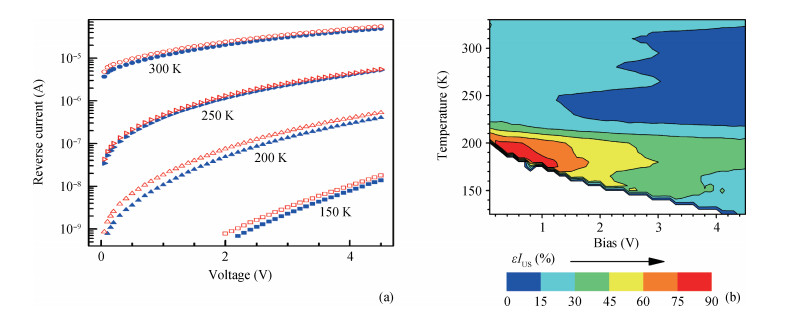
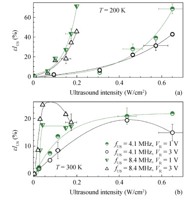
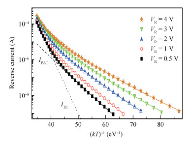
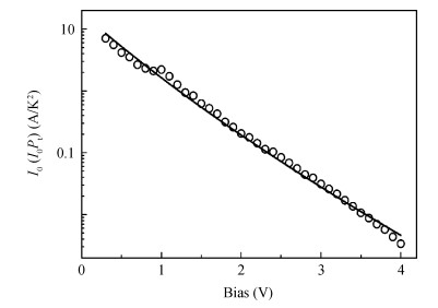
Table 1. Extracted parameters for the Mo/n-Si Schottky structures with and without ultrasonic loading.
 |
| [1] |
Savkina R K, Smirnov A B, Sizov F. The effect of high-frequency sonication on charge carrier transport in LPE and MBE HgCdTe layers. Semicond Sci Technol, 2007, 22(2): 97 doi: 10.1088/0268-1242/22/2/016
|
| [2] |
Kulakova L, Gorelov V, Lutetskiy A, et al. The rotation of the polarization plane of quantum-well heterolasers emission under the ultrasonic strain. Solid State Commun, 2012, 152(17): 1690 doi: 10.1016/j.ssc.2012.04.065
|
| [3] |
Ostrovskii I, Korotchenkov O, Olikh O, et al. Acoustically driven optical phenomena in bulk and low-dimensional semiconductors. J Opt A, 2001, 3(4): S82 https://www.researchgate.net/publication/230991018_Acoustically_driven_optical_phenomena_in_bulk_and_low-dimensional_semiconductors
|
| [4] |
Buyukkose S, Vratzov B, van der Veen J, et al. Ultrahighfrequency surface acoustic wave generation for acoustic charge transport in silicon. Appl Phys Lett, 2013, 102(1): 013112 doi: 10.1063/1.4774388
|
| [5] |
He J H, Gao J, Guo H Z. Correlated electron transport assisted by surface acoustic waves in micron-separated quasi-onedimensional channels. Appl Phys Lett, 2010, 97(12): 122107 doi: 10.1063/1.3491287
|
| [6] |
Ostapenko S S, L Jastrzebski, Sopori B. Change of minority carrier diffusion length in polycrystalline silicon by ultrasound treatment. Semicond Sci Technol, 1995, 10(11): 1494 doi: 10.1088/0268-1242/10/11/011
|
| [7] |
Ostapenko S. Defect passivation using ultrasound treatment: fundamentals and application. Appl Phys A: Mater Sci Process, 1999, 69(2): 225 doi: 10.1007/s003390050994
|
| [8] |
Sukach A, Teterkin V. Ultrasonic treatment-induced modification of the electrical properties of InAs p-n junctions. Tech Phys Lett, 2009, 35(6): 514 doi: 10.1134/S1063785009060108
|
| [9] |
Olikh O. Features of dynamic acoustically induced modification of photovoltaic parameters of silicon solar cells. Semiconductors, 2011, 45(6): 798 doi: 10.1134/S1063782611060170
|
| [10] |
Davletova A, Karazhanov S Z. A study of electrical properties of dislocation engineered Si processed by ultrasound. J Phys Chem Solids, 2009, 70(6): 989 doi: 10.1016/j.jpcs.2009.05.009
|
| [11] |
Davletova A, Karazhanov S Z. Open-circuit voltage decay transient in dislocation-engineered Si p-n junction. J Phys D: Appl Phys, 2008, 41(16): 165107 doi: 10.1088/0022-3727/41/16/165107
|
| [12] |
Melnik V, Olikh Y, Popov V, et al. Characteristics of silicon p-n junction formed by ion implantation with in situ ultrasound treatment. Mater Sci Eng B, 2005, 124/125: 327 doi: 10.1016/j.mseb.2005.08.039
|
| [13] |
Olikh O. Effect of ultrasonic loading on current in Mo/n-n+-Si with Schottky barriers. Semiconductors, 2013, 47(7): 987 doi: 10.1134/S106378261307018X
|
| [14] |
Olikh O. Reversible influence of ultrasound on γ-irradiated Mo/n-Si Schottky barrier structure. Ultrasonics, 2015, 56: 545 doi: 10.1016/j.ultras.2014.10.008
|
| [15] |
Zaveryukhina N, Zaveryukhina E, Vlasov S, et al. Acoustostimulated changes in the density of surface states and their energy spectrum in p-type silicon single crystals. Tech Phys Lett, 2008, 34(3): 241 doi: 10.1134/S106378500803019X
|
| [16] |
Mirsagatov S A, Sapaeva I B, Nazarov Z. Ultrasonic annealing of surface states in the heterojunction of a p-Si/n-CdS/n+-CdS injection photodiode. Inorg Mater, 2015, 51(1): 1 doi: 10.1134/S0020168515010148
|
| [17] |
Wosinski T, Makosa A, Witczak Z. Transformation of native defects in bulk GaAs under ultrasonic vibration. Semicond Sci Technol, 1994, 9(11): 2047 doi: 10.1088/0268-1242/9/11/003
|
| [18] |
Buyanova I A, Ostapenko S S, Sheinkman M K, et al. Ultrasound regeneration of EL2 centres in GaAs. Semicond Sci Technol, 1994, 9(2): 158 doi: 10.1088/0268-1242/9/2/005
|
| [19] |
Korotchenkov O, Grimmliss H. Long-wavelength acousticmode-enhanced electron emission from Se and Te donors in silicon. Phys Rev B, 1995, 52(20): 14598 doi: 10.1103/PhysRevB.52.14598
|
| [20] |
Ostapenko S S, Bell R E. Ultrasound stimulated dissociation of Fe-B pairs in silicon. J Appl Phys, 1995, 77(10): 5458 doi: 10.1063/1.359243
|
| [21] |
Sathaiya D M, Karmalkar S. Thermionic trap-assisted tunneling model and its application to leakage current in nitrided oxides and AlGaN/GaN high electron mobility transistors. J Appl Phys, 2006, 99(9): 093701 doi: 10.1063/1.2191620
|
| [22] |
Shan Q, Meyaard D S, Dai Q, et al. Transport-mechanism analysis of the reverse leakage current in GaInN light-emitting diodes. Appl Phys Lett, 2011, 99(25): 253506 doi: 10.1063/1.3668104
|
| [23] |
Pipinys P, Lapeika V. Temperature dependence of reverse-bias leakage current in GaN Schottky diodes as a consequence of phonon-assisted tunneling. J Appl Phys, 2006, 99(9): 093709 doi: 10.1063/1.2199980
|
| [24] |
Liang Huaguo, Xu Hui, Huang Zhengfeng, et al. Low-leakage and NBTI-mitigated N-type domino logic. Journal of Semiconductors, 2014, 35(1): 015009 doi: 10.1088/1674-4926/35/1/015009
|
| [25] |
Bi Xiuwen, Liang Hailian, Gu Xiaofeng, et al. Design of novel DDSCR with embedded PNP structure for ESD protection. Journal of Semiconductors, 2015, 36(12): 124007 doi: 10.1088/1674-4926/36/12/124007
|
| [26] |
Abu-Samaha F S, Darwish A A A, Mansour A N. Temperature dependent of the current-voltage (Ⅳ) characteristics of TaSi2/nSi structure. Mater Sci Semicond Process, 2013, 16(6): 1988 doi: 10.1016/j.mssp.2013.07.036
|
| [27] |
Jafar M M A G. High-bias current-voltage-temperature characteristics of undoped RF magnetron sputter deposited boron carbide (B5C)/p-type crystalline silicon heterojunctions. Semicond Sci Technol, 2003, 18(1): 7 doi: 10.1088/0268-1242/18/1/302
|
| [28] |
Lee C H, Lim K S. Carrier transport through boron-doped amorphous diamond-like carbon p layer of amorphous silicon based p-i-n solar cells. Appl Phys Lett, 1999, 75(4): 569 doi: 10.1063/1.124444
|
| [29] |
Pipinys P, Pipiniene A, Rimeika A. Phonon-assisted tunneling in reverse biased Schottky diodes. J Appl Phys, 1999, 86(12): 6875 doi: 10.1063/1.371766
|
| [30] |
Tung R T. Recent advances in Schottky barrier concept. Mater Sci Eng, R, 2001, 35(1-3): 1 doi: 10.1016/S0927-796X(01)00037-7
|
| [31] |
Olikh O Y, Voytenko K V, Burbelo R M. Ultrasound influence on I-V-T characteristics of silicon Schottky barrier structure. J Appl Phys, 2015, 117(4): 044505 doi: 10.1063/1.4906844
|
| [32] |
Wang K, Ye M. Parameter determination of Schottky-barrier diode model using differential evolution. Solid-State Electron, 2009, 53(2): 234 doi: 10.1016/j.sse.2008.11.010
|
| [33] |
Rhoderick E H, Williams R H. Metal semiconductor contacts. 2nd ed. Oxford: Clarendon Press, 1988
|
| [34] |
Aboelfotoh M. Electrical characteristics of W-Si(100) Schottky barrier junctions. J Appl Phys, 1989, 66(1): 262 doi: 10.1063/1.343867
|
| [35] |
Zhua S, Meirhaeghea R L V, Detaverniera C, et al. A BEEM study of the temperature dependence of the barrier height distribution in PtSi/n-Si Schottky diodes. Solid State Commun, 1999, 112(11): 611 doi: 10.1016/S0038-1098(99)00404-4
|
| [36] |
Kiveris A, Kudzmauskas S, P P. Release of electrons from traps by an electric field with phonon participation. Phys Stat Sol (a), 1976, 37(1): 321 doi: 10.1002/(ISSN)1521-396X
|
| [37] |
Parker G, McGill T, Mead C, et al. Electric field dependence of GaAs Schottky barriers. Solid-State Electron, 1968, 11(2): 201 doi: 10.1016/0038-1101(68)90079-8
|
| [38] |
Seebauer E G, Kratzer M C. Charged point defects in semiconductors. Mater Sci Eng R, 2006, 55(3-6): 57 doi: 10.1016/j.mser.2006.01.002
|
| [39] |
Lukjanitsa V V. Energy levels of vacancies and interstitial atoms in the band gap of silicon. Semiconductors, 2003, 37(4): 404 doi: 10.1134/1.1568459
|
| [40] |
Mitrofanov O, Manfra M. Poole-Frenkel electron emission from the traps in AlGaN/GaN 13 transistors. J Appl Phys, 2004, 95(11): 6414 doi: 10.1063/1.1719264
|
| [41] |
Zhdanova N G, Kagan M S, Landsberg E G, et al. Ionization of shallow impurities by the electric field in a random coulomb potential. JETP Lett, 1995, 62(2): 119
|
| [42] |
Pavlovich V N. Enhanced diffusion of impurities and defects in crystals in conditions of ultrasonic and radiative excitation of the crystal lattice. Phys Stat Sol (b), 1993, 180(1): 97 doi: 10.1002/(ISSN)1521-3951
|
| [43] |
Mirzade F. Elastic wave propagation in a solid layer with laserinduced point defects. J Appl Phys, 2011, 110(6): 064906 doi: 10.1063/1.3633524
|
| [44] |
Olikh O, Voytenko K. On the mechanism of ultrasonic loading effect in silicon-based Schottky diodes. Ultrasonics, 2016, 66(1): 1
|


Article views: 3328 Times PDF downloads: 18 Times Cited by: 0 Times
Received: 12 February 2016 Revised: 23 June 2016 Online: Published: 01 December 2016
| Citation: |
O.Ya Olikh, K.V. Voitenko, R.M. Burbelo, JaM. Olikh. Effect of ultrasound on reverse leakage current of silicon Schottky barrier structure[J]. Journal of Semiconductors, 2016, 37(12): 122002. doi: 10.1088/1674-4926/37/12/122002
****
O. Y. Olikh, K. V. Voitenko, R. M. Burbelo, J. M. Olikh. Effect of ultrasound on reverse leakage current of silicon Schottky barrier structure[J]. J. Semicond., 2016, 37(12): 122002. doi:? 10.1088/1674-4926/37/12/122002.

|
| [1] |
Savkina R K, Smirnov A B, Sizov F. The effect of high-frequency sonication on charge carrier transport in LPE and MBE HgCdTe layers. Semicond Sci Technol, 2007, 22(2): 97 doi: 10.1088/0268-1242/22/2/016
|
| [2] |
Kulakova L, Gorelov V, Lutetskiy A, et al. The rotation of the polarization plane of quantum-well heterolasers emission under the ultrasonic strain. Solid State Commun, 2012, 152(17): 1690 doi: 10.1016/j.ssc.2012.04.065
|
| [3] |
Ostrovskii I, Korotchenkov O, Olikh O, et al. Acoustically driven optical phenomena in bulk and low-dimensional semiconductors. J Opt A, 2001, 3(4): S82 https://www.researchgate.net/publication/230991018_Acoustically_driven_optical_phenomena_in_bulk_and_low-dimensional_semiconductors
|
| [4] |
Buyukkose S, Vratzov B, van der Veen J, et al. Ultrahighfrequency surface acoustic wave generation for acoustic charge transport in silicon. Appl Phys Lett, 2013, 102(1): 013112 doi: 10.1063/1.4774388
|
| [5] |
He J H, Gao J, Guo H Z. Correlated electron transport assisted by surface acoustic waves in micron-separated quasi-onedimensional channels. Appl Phys Lett, 2010, 97(12): 122107 doi: 10.1063/1.3491287
|
| [6] |
Ostapenko S S, L Jastrzebski, Sopori B. Change of minority carrier diffusion length in polycrystalline silicon by ultrasound treatment. Semicond Sci Technol, 1995, 10(11): 1494 doi: 10.1088/0268-1242/10/11/011
|
| [7] |
Ostapenko S. Defect passivation using ultrasound treatment: fundamentals and application. Appl Phys A: Mater Sci Process, 1999, 69(2): 225 doi: 10.1007/s003390050994
|
| [8] |
Sukach A, Teterkin V. Ultrasonic treatment-induced modification of the electrical properties of InAs p-n junctions. Tech Phys Lett, 2009, 35(6): 514 doi: 10.1134/S1063785009060108
|
| [9] |
Olikh O. Features of dynamic acoustically induced modification of photovoltaic parameters of silicon solar cells. Semiconductors, 2011, 45(6): 798 doi: 10.1134/S1063782611060170
|
| [10] |
Davletova A, Karazhanov S Z. A study of electrical properties of dislocation engineered Si processed by ultrasound. J Phys Chem Solids, 2009, 70(6): 989 doi: 10.1016/j.jpcs.2009.05.009
|
| [11] |
Davletova A, Karazhanov S Z. Open-circuit voltage decay transient in dislocation-engineered Si p-n junction. J Phys D: Appl Phys, 2008, 41(16): 165107 doi: 10.1088/0022-3727/41/16/165107
|
| [12] |
Melnik V, Olikh Y, Popov V, et al. Characteristics of silicon p-n junction formed by ion implantation with in situ ultrasound treatment. Mater Sci Eng B, 2005, 124/125: 327 doi: 10.1016/j.mseb.2005.08.039
|
| [13] |
Olikh O. Effect of ultrasonic loading on current in Mo/n-n+-Si with Schottky barriers. Semiconductors, 2013, 47(7): 987 doi: 10.1134/S106378261307018X
|
| [14] |
Olikh O. Reversible influence of ultrasound on γ-irradiated Mo/n-Si Schottky barrier structure. Ultrasonics, 2015, 56: 545 doi: 10.1016/j.ultras.2014.10.008
|
| [15] |
Zaveryukhina N, Zaveryukhina E, Vlasov S, et al. Acoustostimulated changes in the density of surface states and their energy spectrum in p-type silicon single crystals. Tech Phys Lett, 2008, 34(3): 241 doi: 10.1134/S106378500803019X
|
| [16] |
Mirsagatov S A, Sapaeva I B, Nazarov Z. Ultrasonic annealing of surface states in the heterojunction of a p-Si/n-CdS/n+-CdS injection photodiode. Inorg Mater, 2015, 51(1): 1 doi: 10.1134/S0020168515010148
|
| [17] |
Wosinski T, Makosa A, Witczak Z. Transformation of native defects in bulk GaAs under ultrasonic vibration. Semicond Sci Technol, 1994, 9(11): 2047 doi: 10.1088/0268-1242/9/11/003
|
| [18] |
Buyanova I A, Ostapenko S S, Sheinkman M K, et al. Ultrasound regeneration of EL2 centres in GaAs. Semicond Sci Technol, 1994, 9(2): 158 doi: 10.1088/0268-1242/9/2/005
|
| [19] |
Korotchenkov O, Grimmliss H. Long-wavelength acousticmode-enhanced electron emission from Se and Te donors in silicon. Phys Rev B, 1995, 52(20): 14598 doi: 10.1103/PhysRevB.52.14598
|
| [20] |
Ostapenko S S, Bell R E. Ultrasound stimulated dissociation of Fe-B pairs in silicon. J Appl Phys, 1995, 77(10): 5458 doi: 10.1063/1.359243
|
| [21] |
Sathaiya D M, Karmalkar S. Thermionic trap-assisted tunneling model and its application to leakage current in nitrided oxides and AlGaN/GaN high electron mobility transistors. J Appl Phys, 2006, 99(9): 093701 doi: 10.1063/1.2191620
|
| [22] |
Shan Q, Meyaard D S, Dai Q, et al. Transport-mechanism analysis of the reverse leakage current in GaInN light-emitting diodes. Appl Phys Lett, 2011, 99(25): 253506 doi: 10.1063/1.3668104
|
| [23] |
Pipinys P, Lapeika V. Temperature dependence of reverse-bias leakage current in GaN Schottky diodes as a consequence of phonon-assisted tunneling. J Appl Phys, 2006, 99(9): 093709 doi: 10.1063/1.2199980
|
| [24] |
Liang Huaguo, Xu Hui, Huang Zhengfeng, et al. Low-leakage and NBTI-mitigated N-type domino logic. Journal of Semiconductors, 2014, 35(1): 015009 doi: 10.1088/1674-4926/35/1/015009
|
| [25] |
Bi Xiuwen, Liang Hailian, Gu Xiaofeng, et al. Design of novel DDSCR with embedded PNP structure for ESD protection. Journal of Semiconductors, 2015, 36(12): 124007 doi: 10.1088/1674-4926/36/12/124007
|
| [26] |
Abu-Samaha F S, Darwish A A A, Mansour A N. Temperature dependent of the current-voltage (Ⅳ) characteristics of TaSi2/nSi structure. Mater Sci Semicond Process, 2013, 16(6): 1988 doi: 10.1016/j.mssp.2013.07.036
|
| [27] |
Jafar M M A G. High-bias current-voltage-temperature characteristics of undoped RF magnetron sputter deposited boron carbide (B5C)/p-type crystalline silicon heterojunctions. Semicond Sci Technol, 2003, 18(1): 7 doi: 10.1088/0268-1242/18/1/302
|
| [28] |
Lee C H, Lim K S. Carrier transport through boron-doped amorphous diamond-like carbon p layer of amorphous silicon based p-i-n solar cells. Appl Phys Lett, 1999, 75(4): 569 doi: 10.1063/1.124444
|
| [29] |
Pipinys P, Pipiniene A, Rimeika A. Phonon-assisted tunneling in reverse biased Schottky diodes. J Appl Phys, 1999, 86(12): 6875 doi: 10.1063/1.371766
|
| [30] |
Tung R T. Recent advances in Schottky barrier concept. Mater Sci Eng, R, 2001, 35(1-3): 1 doi: 10.1016/S0927-796X(01)00037-7
|
| [31] |
Olikh O Y, Voytenko K V, Burbelo R M. Ultrasound influence on I-V-T characteristics of silicon Schottky barrier structure. J Appl Phys, 2015, 117(4): 044505 doi: 10.1063/1.4906844
|
| [32] |
Wang K, Ye M. Parameter determination of Schottky-barrier diode model using differential evolution. Solid-State Electron, 2009, 53(2): 234 doi: 10.1016/j.sse.2008.11.010
|
| [33] |
Rhoderick E H, Williams R H. Metal semiconductor contacts. 2nd ed. Oxford: Clarendon Press, 1988
|
| [34] |
Aboelfotoh M. Electrical characteristics of W-Si(100) Schottky barrier junctions. J Appl Phys, 1989, 66(1): 262 doi: 10.1063/1.343867
|
| [35] |
Zhua S, Meirhaeghea R L V, Detaverniera C, et al. A BEEM study of the temperature dependence of the barrier height distribution in PtSi/n-Si Schottky diodes. Solid State Commun, 1999, 112(11): 611 doi: 10.1016/S0038-1098(99)00404-4
|
| [36] |
Kiveris A, Kudzmauskas S, P P. Release of electrons from traps by an electric field with phonon participation. Phys Stat Sol (a), 1976, 37(1): 321 doi: 10.1002/(ISSN)1521-396X
|
| [37] |
Parker G, McGill T, Mead C, et al. Electric field dependence of GaAs Schottky barriers. Solid-State Electron, 1968, 11(2): 201 doi: 10.1016/0038-1101(68)90079-8
|
| [38] |
Seebauer E G, Kratzer M C. Charged point defects in semiconductors. Mater Sci Eng R, 2006, 55(3-6): 57 doi: 10.1016/j.mser.2006.01.002
|
| [39] |
Lukjanitsa V V. Energy levels of vacancies and interstitial atoms in the band gap of silicon. Semiconductors, 2003, 37(4): 404 doi: 10.1134/1.1568459
|
| [40] |
Mitrofanov O, Manfra M. Poole-Frenkel electron emission from the traps in AlGaN/GaN 13 transistors. J Appl Phys, 2004, 95(11): 6414 doi: 10.1063/1.1719264
|
| [41] |
Zhdanova N G, Kagan M S, Landsberg E G, et al. Ionization of shallow impurities by the electric field in a random coulomb potential. JETP Lett, 1995, 62(2): 119
|
| [42] |
Pavlovich V N. Enhanced diffusion of impurities and defects in crystals in conditions of ultrasonic and radiative excitation of the crystal lattice. Phys Stat Sol (b), 1993, 180(1): 97 doi: 10.1002/(ISSN)1521-3951
|
| [43] |
Mirzade F. Elastic wave propagation in a solid layer with laserinduced point defects. J Appl Phys, 2011, 110(6): 064906 doi: 10.1063/1.3633524
|
| [44] |
Olikh O, Voytenko K. On the mechanism of ultrasonic loading effect in silicon-based Schottky diodes. Ultrasonics, 2016, 66(1): 1
|

 WeChat ID
Journal of Semiconductors © 2017 All Rights Reserved 京ICP備05085259號-2
 DownLoad:

