


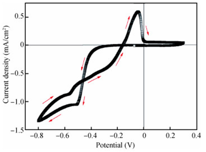
Fig. 1.
The cyclic voltammogram from aqueous solution containing 0.05 M Cu sulfate and 0.05 M C6H8O7 at pH of 6 and scan rate of 20 mV/s.
SEMICONDUCTOR MATERIALS
D. Mohra1, M. Benhaliliba1, , M. Serin2, M.R. Khelladi3, H. Lahmar3 and A. Azizi3
Corresponding author: M. Benhaliliba, Email: mbenhaliliba@gmail.com
Abstract: The thin films of Cu2O are deposited by electrodeposition technique onto indium tin oxide (ITO)-coated glass substrate at different potentials. The precursor is an aqueous solution which contains respectively 0.05 M of CuSO4 and citric acid at kept temperature of 60℃ and the applied potential varies within the {-0.4 V,-0.7 V} SCE range. Based on the chronocoulometry (CC) process, the electrochemical, structural and optical parameters are determined. We measured the current as function of potential within the {-0.4 V,-0.7 V} range and the higher current is found to be within the {-0.7 V,-0.3 V} band. The grain sizes are of 12.12 nm and 35.47 nm according to (110) and (221) orientations respectively. The high textural coefficient of 0.943 is recorded for the potential-0.7 V. The transmittance of 72.25 %, within the visible band, is obtained for the as-grown layer at-0.4 V and the band gap is found to be 2.2 eV for the electrodeposition potential of-0.7 V.
Key words: Cu2O films, chronocoulometry, electrodeposition, ITO substrate, voltammogram, cathodic potential
| [1] |
?Chatterjee S, Sudip K S, Amlan J P. Formation of all-oxide solar cells in atmospheric condition based on Cu2O thin-films grown through SILAR technique. Solar Energy Materials & Solar Cells, 2016, 147: 17
|
| [2] |
Hsueh H T, Chang S J, Hung F Y, et al. Fabrication of coaxial p-Cu2O/n-ZnO nanowire photodiodes. Superlattices and Microstructures, 2011, 49: 572 doi: 10.1016/j.spmi.2011.03.011
|
| [3] |
Wang L C, De Tacconi N R, Chenthamarakshan C R, et al. Electrodeposition copper oxide films: effect of bath pH on grain orientation and orientation-dependant interfacial behavior. Thin Solid Films, 2007, 515: 3090 doi: 10.1016/j.tsf.2006.08.041
|
| [4] |
Pan F, Gao S, Chen C, et al. Recent progress in resistive random access memories: materials, switching mechanisms, and performance. Materials Science and Engineering R, 2004, 83: 1 http://cn.bing.com/academic/profile?id=2034876082&encoded=0&v=paper_preview&mkt=zh-cn
|
| [5] |
Zhang Z, Hu W, Zhong Y C, et al. The effect of complexing agents on the oriented growth of electrodeposited microcrystalline cuprous oxide film. Materials Research Bulletin, 2012, 47: 2561 doi: 10.1016/j.materresbull.2012.04.146
|
| [6] |
Al-Kuhaili M F. Characterization of copper oxide thin films deposited by the thermal evaporation of cuprous oxide (Cu2O). Vacuum, 2008, 82: 623 doi: 10.1016/j.vacuum.2007.10.004
|
| [7] |
Laia G, Wub Y, Linb L, et al. Low resistivity of N-doped Cu2O thin films deposited by RF-magnetron sputtering. Applied Surface Science, 2013, 285: 755 doi: 10.1016/j.apsusc.2013.08.122
|
| [8] |
Kayani Z N, Ali Y, Kiran F, et al. Fabrication of copper oxide nanoparticles by sol-gel route. Materials Today: Proceedings, 2015, 2: 5446 doi: 10.1016/j.matpr.2015.11.067
|
| [9] |
Kasmi A, Yu Tian Z, Vieker H, et al. Innovative CVD synthesis of Cu2O catalysts for CO oxidation. Applied Catalysis B, 2016, 186: 10 doi: 10.1016/j.apcatb.2015.12.034
|
| [10] |
Lva J, Xua J, Zhao M, et al. Effect of seed layer on optical properties and visible photoresponse of ZnO/Cu2O composite thin films. Ceramics International, 2015, 41: 13983 doi: 10.1016/j.ceramint.2015.07.010
|
| [11] |
Yan D, Li S, Hu M, et al. Electrochemical synthesis and the gas sensing properties of the Cu2O nanofilms/porous silicon hybrid structure. Sensors and Actuators B, 2016, 223: 626 doi: 10.1016/j.snb.2015.09.080
|
| [12] |
Khelladi M R, Mentar L, Benaiche A, et al. A study on electrodeposited zinc oxide nanostructures. J Mater Sci: Mater Electron, 2013 24: 153 doi: 10.1007/s10854-012-0973-5
|
| [13] |
Meng H, Yang W, Yan X, et al. A highly sensitive and fast responsive semiconductor metal oxide detector based on In2O3 nanoparticle film for portable gas chromatograph. Sensors and Actuators B, 2015, 216: 511 doi: 10.1016/j.snb.2015.04.068
|
| [14] |
Benhaliliba M, Benouis C E, Yakuphanoglu F, et al. Detailed investigation of submicrometer-sized grains of chemically sprayed (Sn1-xAlx, O2) (0 ≤qslant x ≤qslant 0.085) thin films. Journal of Alloys and Compounds, 2012, 527: 40 doi: 10.1016/j.jallcom.2012.02.128
|
| [15] |
Jiang S, Wu M, Zhou Y, et al. Effects of electrodeposition conditions on the microstructures of ZnO thin films. Integrated Ferroelectrics, 2007, 88: 33 doi: 10.1080/10584580601098563
|
| [16] |
Bard A J, Faulkner L R. Electrochemical methods: fundamentals and applications. Wiley, 2001
|
| [17] |
Wang L, Tao M. Fabrication and characterization of p-n homojunction in cuprous oxide by electrochemical deposition. Electrochem Solid State Lett, 2007, 10: 248 doi: 10.1149/1.2748632
|
| [18] |
Laidoudi S, Bioud A Y, Azizi A, et al. Growth and characterization of electrodeposited Cu2O thin films. Semicond Sci Technol, 2013, 28: 115005 doi: 10.1088/0268-1242/28/11/115005
|
| [19] |
Chatterjee A P, Mukhopadhyay A K, Chakraborty A K, et al. Electrodeposition and characterization of cuprous oxide films. Materials Letters, 1991, 11: 10 doi: 10.1016/0167-577X(91)90180-E
|
| [20] |
Lee Y H, Leu I C, Liao C L, et al. The structural evolution and electrochemical properties of the textured Cu2O thin films. Journal of Alloys and Compounds, 2007, 436: 241 doi: 10.1016/j.jallcom.2006.07.019
|
| [21] |
Hsu Y K , Wu J R, Chen M H, et al. Fabrication of homojunction Cu2O solar cells by electrochemical deposition. Applied Surface Science, 2015, 354: 8 doi: 10.1016/j.apsusc.2015.05.142
|
| [22] |
No Y S, Oh D H, Su K S, et al. Structural, optical, and electrical properties of Cu2O nanocubes grown on indium-tin-oxide-coated glass substrates by using seed-layer-free electrochemical deposition method. Applied Surface Science, 2012, 258: 7581 doi: 10.1016/j.apsusc.2012.04.091
|
| [23] |
Benhaliliba M, Benouis C E, Tiburcio-Silver A. Low copper doped CdO nanowires grown by sol-gel route. Journal of New Technology and Materials, 2011, 1: 24 https://www.researchgate.net/publication/256117103_Low_Copper_Doped_CdO_Nanowires_Grown_by_Sol-Gel_Route
|
| [24] |
Messaoudi O, Makhlouf H, Souissi A, et al. Correlation between optical and structural properties of copper oxide electrodeposited on ITO glass. Journal of Alloys and Compounds, 2014, 611: 142 doi: 10.1016/j.jallcom.2014.05.055
|
| [25] |
Tounsi N, Barhoumi A, Akkari F C, et al. Structural and optical characterization of copper oxide composite thin films elaborated by GLAD technique. Vacuum, 2015, 121: 9 doi: 10.1016/j.vacuum.2015.07.011
|
| [26] |
Kim M S, Kim D Y, Cho M Y, et al. Effects of buffer layer thickness on properties of ZnO thin films grown on porous silicon by plasma-assisted molecular beam epitaxy. Vacuum, 2012, 86: 1373 doi: 10.1016/j.vacuum.2012.01.006
|
| [27] |
Zhang D K, Liu Y C, Liu Y L, et al. The electrical properties and the interfaces of Cu2O/ZnO/ITO p-i-n heterojunction. Physica B, 2004, 351: 178 doi: 10.1016/j.physb.2004.06.003
|
| [28] |
Han K. Electrodeposited cuprous oxide solar cells. The University of Texas At Arlington, December 2009
|
| [29] |
Tombak A, Benhaliliba M, Ocak Y S, et al. The novel transparent sputtered p-type CuO thin films and Ag/p-CuO/n-Si Schottky diode applications. Results in Physics, 2015, 5: 314 doi: 10.1016/j.rinp.2015.11.001
|
| [30] |
Benouis C E, Benhaliliba M, Yakuphanoglu F, et al. Physical properties of ultrasonic sprayed nanosized indium doped SnO2 films. Synthetic Metals, 2011, 161: 1509 doi: 10.1016/j.synthmet.2011.04.017
|
| [31] |
Brandt I S, Martins C A, Zoldan V C, et al. Structural and optical properties of Cu2O crystalline electrodeposited films. Thin Solid Films, 2014, 562: 144 doi: 10.1016/j.tsf.2014.04.013
|
| [32] |
Ravindra N M, Srivastava V K. Variation of refractive index with energy gap in semiconductors. Infrared Phys, 1979, 19: 603 doi: 10.1016/0020-0891(79)90081-2
|
| [33] |
Gupta V P, Ravindra N M. Comments on the moss formula. Phys Stat Sol B, 1980, 100: 715 doi: 10.1002/(ISSN)1521-3951
|
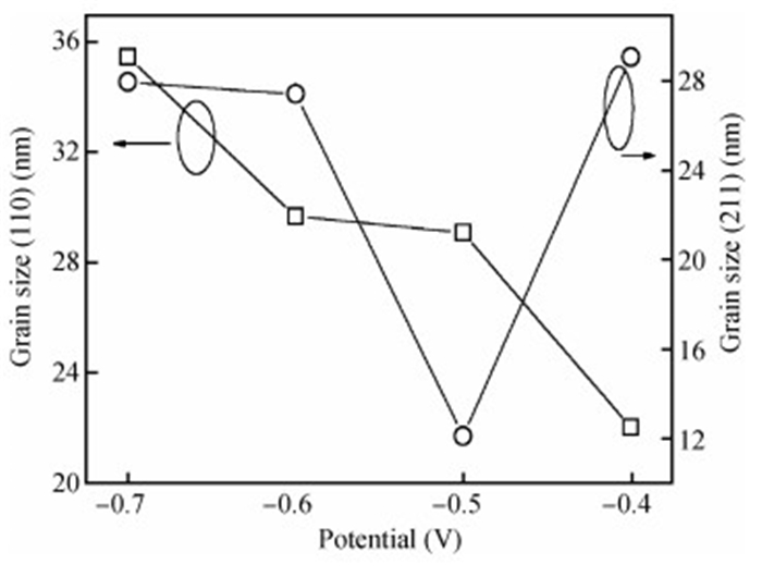
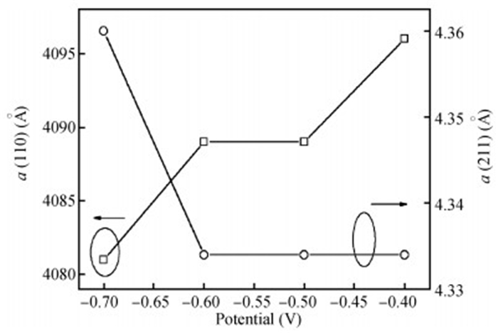
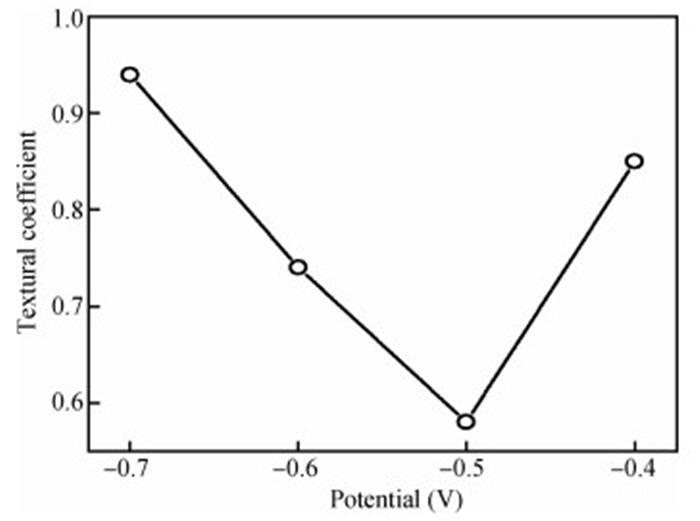
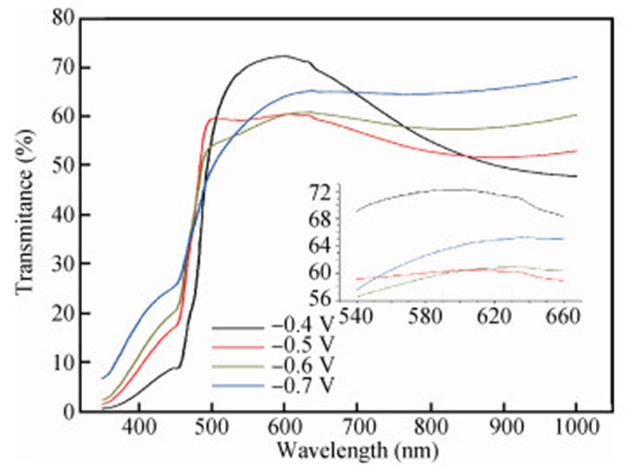
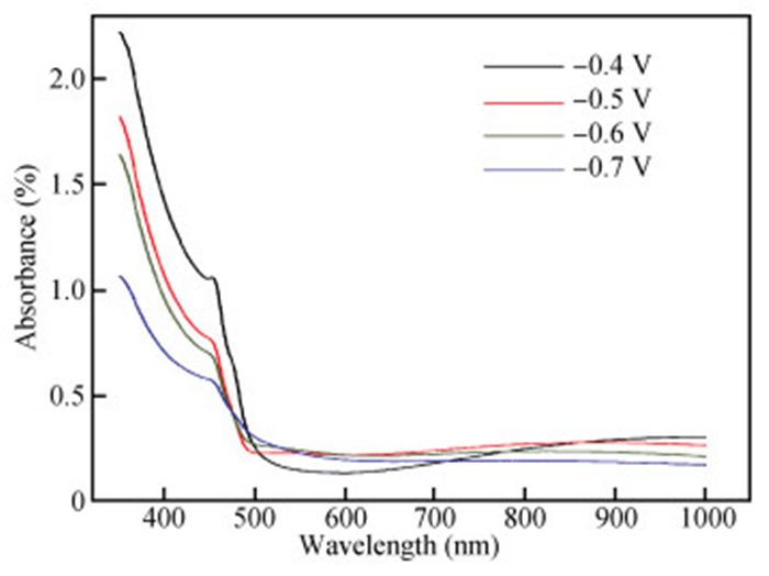
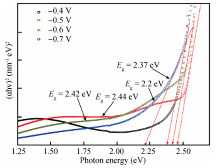
Table 1. The calculated structural parameters of (110) planes of the electrodeposited Cu2O/ITO thin films.

|
Table 2. The calculated structural parameters of (211) planes of the electrodeposited Cu2O/ITO thin films.

|
Table 3. Optical parameters of Cu2O/ITO layers grown at different potentials.

|
| [1] |
?Chatterjee S, Sudip K S, Amlan J P. Formation of all-oxide solar cells in atmospheric condition based on Cu2O thin-films grown through SILAR technique. Solar Energy Materials & Solar Cells, 2016, 147: 17
|
| [2] |
Hsueh H T, Chang S J, Hung F Y, et al. Fabrication of coaxial p-Cu2O/n-ZnO nanowire photodiodes. Superlattices and Microstructures, 2011, 49: 572 doi: 10.1016/j.spmi.2011.03.011
|
| [3] |
Wang L C, De Tacconi N R, Chenthamarakshan C R, et al. Electrodeposition copper oxide films: effect of bath pH on grain orientation and orientation-dependant interfacial behavior. Thin Solid Films, 2007, 515: 3090 doi: 10.1016/j.tsf.2006.08.041
|
| [4] |
Pan F, Gao S, Chen C, et al. Recent progress in resistive random access memories: materials, switching mechanisms, and performance. Materials Science and Engineering R, 2004, 83: 1 http://cn.bing.com/academic/profile?id=2034876082&encoded=0&v=paper_preview&mkt=zh-cn
|
| [5] |
Zhang Z, Hu W, Zhong Y C, et al. The effect of complexing agents on the oriented growth of electrodeposited microcrystalline cuprous oxide film. Materials Research Bulletin, 2012, 47: 2561 doi: 10.1016/j.materresbull.2012.04.146
|
| [6] |
Al-Kuhaili M F. Characterization of copper oxide thin films deposited by the thermal evaporation of cuprous oxide (Cu2O). Vacuum, 2008, 82: 623 doi: 10.1016/j.vacuum.2007.10.004
|
| [7] |
Laia G, Wub Y, Linb L, et al. Low resistivity of N-doped Cu2O thin films deposited by RF-magnetron sputtering. Applied Surface Science, 2013, 285: 755 doi: 10.1016/j.apsusc.2013.08.122
|
| [8] |
Kayani Z N, Ali Y, Kiran F, et al. Fabrication of copper oxide nanoparticles by sol-gel route. Materials Today: Proceedings, 2015, 2: 5446 doi: 10.1016/j.matpr.2015.11.067
|
| [9] |
Kasmi A, Yu Tian Z, Vieker H, et al. Innovative CVD synthesis of Cu2O catalysts for CO oxidation. Applied Catalysis B, 2016, 186: 10 doi: 10.1016/j.apcatb.2015.12.034
|
| [10] |
Lva J, Xua J, Zhao M, et al. Effect of seed layer on optical properties and visible photoresponse of ZnO/Cu2O composite thin films. Ceramics International, 2015, 41: 13983 doi: 10.1016/j.ceramint.2015.07.010
|
| [11] |
Yan D, Li S, Hu M, et al. Electrochemical synthesis and the gas sensing properties of the Cu2O nanofilms/porous silicon hybrid structure. Sensors and Actuators B, 2016, 223: 626 doi: 10.1016/j.snb.2015.09.080
|
| [12] |
Khelladi M R, Mentar L, Benaiche A, et al. A study on electrodeposited zinc oxide nanostructures. J Mater Sci: Mater Electron, 2013 24: 153 doi: 10.1007/s10854-012-0973-5
|
| [13] |
Meng H, Yang W, Yan X, et al. A highly sensitive and fast responsive semiconductor metal oxide detector based on In2O3 nanoparticle film for portable gas chromatograph. Sensors and Actuators B, 2015, 216: 511 doi: 10.1016/j.snb.2015.04.068
|
| [14] |
Benhaliliba M, Benouis C E, Yakuphanoglu F, et al. Detailed investigation of submicrometer-sized grains of chemically sprayed (Sn1-xAlx, O2) (0 ≤qslant x ≤qslant 0.085) thin films. Journal of Alloys and Compounds, 2012, 527: 40 doi: 10.1016/j.jallcom.2012.02.128
|
| [15] |
Jiang S, Wu M, Zhou Y, et al. Effects of electrodeposition conditions on the microstructures of ZnO thin films. Integrated Ferroelectrics, 2007, 88: 33 doi: 10.1080/10584580601098563
|
| [16] |
Bard A J, Faulkner L R. Electrochemical methods: fundamentals and applications. Wiley, 2001
|
| [17] |
Wang L, Tao M. Fabrication and characterization of p-n homojunction in cuprous oxide by electrochemical deposition. Electrochem Solid State Lett, 2007, 10: 248 doi: 10.1149/1.2748632
|
| [18] |
Laidoudi S, Bioud A Y, Azizi A, et al. Growth and characterization of electrodeposited Cu2O thin films. Semicond Sci Technol, 2013, 28: 115005 doi: 10.1088/0268-1242/28/11/115005
|
| [19] |
Chatterjee A P, Mukhopadhyay A K, Chakraborty A K, et al. Electrodeposition and characterization of cuprous oxide films. Materials Letters, 1991, 11: 10 doi: 10.1016/0167-577X(91)90180-E
|
| [20] |
Lee Y H, Leu I C, Liao C L, et al. The structural evolution and electrochemical properties of the textured Cu2O thin films. Journal of Alloys and Compounds, 2007, 436: 241 doi: 10.1016/j.jallcom.2006.07.019
|
| [21] |
Hsu Y K , Wu J R, Chen M H, et al. Fabrication of homojunction Cu2O solar cells by electrochemical deposition. Applied Surface Science, 2015, 354: 8 doi: 10.1016/j.apsusc.2015.05.142
|
| [22] |
No Y S, Oh D H, Su K S, et al. Structural, optical, and electrical properties of Cu2O nanocubes grown on indium-tin-oxide-coated glass substrates by using seed-layer-free electrochemical deposition method. Applied Surface Science, 2012, 258: 7581 doi: 10.1016/j.apsusc.2012.04.091
|
| [23] |
Benhaliliba M, Benouis C E, Tiburcio-Silver A. Low copper doped CdO nanowires grown by sol-gel route. Journal of New Technology and Materials, 2011, 1: 24 https://www.researchgate.net/publication/256117103_Low_Copper_Doped_CdO_Nanowires_Grown_by_Sol-Gel_Route
|
| [24] |
Messaoudi O, Makhlouf H, Souissi A, et al. Correlation between optical and structural properties of copper oxide electrodeposited on ITO glass. Journal of Alloys and Compounds, 2014, 611: 142 doi: 10.1016/j.jallcom.2014.05.055
|
| [25] |
Tounsi N, Barhoumi A, Akkari F C, et al. Structural and optical characterization of copper oxide composite thin films elaborated by GLAD technique. Vacuum, 2015, 121: 9 doi: 10.1016/j.vacuum.2015.07.011
|
| [26] |
Kim M S, Kim D Y, Cho M Y, et al. Effects of buffer layer thickness on properties of ZnO thin films grown on porous silicon by plasma-assisted molecular beam epitaxy. Vacuum, 2012, 86: 1373 doi: 10.1016/j.vacuum.2012.01.006
|
| [27] |
Zhang D K, Liu Y C, Liu Y L, et al. The electrical properties and the interfaces of Cu2O/ZnO/ITO p-i-n heterojunction. Physica B, 2004, 351: 178 doi: 10.1016/j.physb.2004.06.003
|
| [28] |
Han K. Electrodeposited cuprous oxide solar cells. The University of Texas At Arlington, December 2009
|
| [29] |
Tombak A, Benhaliliba M, Ocak Y S, et al. The novel transparent sputtered p-type CuO thin films and Ag/p-CuO/n-Si Schottky diode applications. Results in Physics, 2015, 5: 314 doi: 10.1016/j.rinp.2015.11.001
|
| [30] |
Benouis C E, Benhaliliba M, Yakuphanoglu F, et al. Physical properties of ultrasonic sprayed nanosized indium doped SnO2 films. Synthetic Metals, 2011, 161: 1509 doi: 10.1016/j.synthmet.2011.04.017
|
| [31] |
Brandt I S, Martins C A, Zoldan V C, et al. Structural and optical properties of Cu2O crystalline electrodeposited films. Thin Solid Films, 2014, 562: 144 doi: 10.1016/j.tsf.2014.04.013
|
| [32] |
Ravindra N M, Srivastava V K. Variation of refractive index with energy gap in semiconductors. Infrared Phys, 1979, 19: 603 doi: 10.1016/0020-0891(79)90081-2
|
| [33] |
Gupta V P, Ravindra N M. Comments on the moss formula. Phys Stat Sol B, 1980, 100: 715 doi: 10.1002/(ISSN)1521-3951
|


Article views: 3604 Times PDF downloads: 52 Times Cited by: 0 Times
Received: 17 February 2016 Revised: 18 May 2016 Online: Published: 01 October 2016
| Citation: |
D. Mohra, M. Benhaliliba, M. Serin, M.R. Khelladi, H. Lahmar, A. Azizi. The investigation of electrodeposited Cu2O/ITO layers by chronocoulometry process: effect of electrical potential[J]. Journal of Semiconductors, 2016, 37(10): 103001. doi: 10.1088/1674-4926/37/10/103001
****
D. Mohra, M. Benhaliliba, M. Serin, M.R. Khelladi, H. Lahmar, A. Azizi. The investigation of electrodeposited Cu2O/ITO layers by chronocoulometry process: effect of electrical potential[J]. J. Semicond., 2016, 37(10): 103001. doi: 10.1088/1674-4926/37/10/103001.

|
Scientific Research Projects Coordination 2012-01-01-KAP05
PNR 8/U311/R77
National Administration of Scientific Research, the CNEPRU of Oran University of Sciences and Technology B00L02UN310220130011
Scientific Research Projects Coordination 2012-01-01-KAP06
PNR U311/R81
Project supported the PNR (Nos. 8/U311/R77, U311/R81), the “Agencethematique de rechercheen science ettechnologie” (ATRST), the National Administration of Scientific Research, the CNEPRU of Oran University of Sciences and Technology (No. B00L02UN310220130011), and the Scientific Research Projects Coordination (Nos. 2012-01-01-KAP05, 2012-01-01-KAP06) Yildiz Technical University.
| [1] |
?Chatterjee S, Sudip K S, Amlan J P. Formation of all-oxide solar cells in atmospheric condition based on Cu2O thin-films grown through SILAR technique. Solar Energy Materials & Solar Cells, 2016, 147: 17
|
| [2] |
Hsueh H T, Chang S J, Hung F Y, et al. Fabrication of coaxial p-Cu2O/n-ZnO nanowire photodiodes. Superlattices and Microstructures, 2011, 49: 572 doi: 10.1016/j.spmi.2011.03.011
|
| [3] |
Wang L C, De Tacconi N R, Chenthamarakshan C R, et al. Electrodeposition copper oxide films: effect of bath pH on grain orientation and orientation-dependant interfacial behavior. Thin Solid Films, 2007, 515: 3090 doi: 10.1016/j.tsf.2006.08.041
|
| [4] |
Pan F, Gao S, Chen C, et al. Recent progress in resistive random access memories: materials, switching mechanisms, and performance. Materials Science and Engineering R, 2004, 83: 1 http://cn.bing.com/academic/profile?id=2034876082&encoded=0&v=paper_preview&mkt=zh-cn
|
| [5] |
Zhang Z, Hu W, Zhong Y C, et al. The effect of complexing agents on the oriented growth of electrodeposited microcrystalline cuprous oxide film. Materials Research Bulletin, 2012, 47: 2561 doi: 10.1016/j.materresbull.2012.04.146
|
| [6] |
Al-Kuhaili M F. Characterization of copper oxide thin films deposited by the thermal evaporation of cuprous oxide (Cu2O). Vacuum, 2008, 82: 623 doi: 10.1016/j.vacuum.2007.10.004
|
| [7] |
Laia G, Wub Y, Linb L, et al. Low resistivity of N-doped Cu2O thin films deposited by RF-magnetron sputtering. Applied Surface Science, 2013, 285: 755 doi: 10.1016/j.apsusc.2013.08.122
|
| [8] |
Kayani Z N, Ali Y, Kiran F, et al. Fabrication of copper oxide nanoparticles by sol-gel route. Materials Today: Proceedings, 2015, 2: 5446 doi: 10.1016/j.matpr.2015.11.067
|
| [9] |
Kasmi A, Yu Tian Z, Vieker H, et al. Innovative CVD synthesis of Cu2O catalysts for CO oxidation. Applied Catalysis B, 2016, 186: 10 doi: 10.1016/j.apcatb.2015.12.034
|
| [10] |
Lva J, Xua J, Zhao M, et al. Effect of seed layer on optical properties and visible photoresponse of ZnO/Cu2O composite thin films. Ceramics International, 2015, 41: 13983 doi: 10.1016/j.ceramint.2015.07.010
|
| [11] |
Yan D, Li S, Hu M, et al. Electrochemical synthesis and the gas sensing properties of the Cu2O nanofilms/porous silicon hybrid structure. Sensors and Actuators B, 2016, 223: 626 doi: 10.1016/j.snb.2015.09.080
|
| [12] |
Khelladi M R, Mentar L, Benaiche A, et al. A study on electrodeposited zinc oxide nanostructures. J Mater Sci: Mater Electron, 2013 24: 153 doi: 10.1007/s10854-012-0973-5
|
| [13] |
Meng H, Yang W, Yan X, et al. A highly sensitive and fast responsive semiconductor metal oxide detector based on In2O3 nanoparticle film for portable gas chromatograph. Sensors and Actuators B, 2015, 216: 511 doi: 10.1016/j.snb.2015.04.068
|
| [14] |
Benhaliliba M, Benouis C E, Yakuphanoglu F, et al. Detailed investigation of submicrometer-sized grains of chemically sprayed (Sn1-xAlx, O2) (0 ≤qslant x ≤qslant 0.085) thin films. Journal of Alloys and Compounds, 2012, 527: 40 doi: 10.1016/j.jallcom.2012.02.128
|
| [15] |
Jiang S, Wu M, Zhou Y, et al. Effects of electrodeposition conditions on the microstructures of ZnO thin films. Integrated Ferroelectrics, 2007, 88: 33 doi: 10.1080/10584580601098563
|
| [16] |
Bard A J, Faulkner L R. Electrochemical methods: fundamentals and applications. Wiley, 2001
|
| [17] |
Wang L, Tao M. Fabrication and characterization of p-n homojunction in cuprous oxide by electrochemical deposition. Electrochem Solid State Lett, 2007, 10: 248 doi: 10.1149/1.2748632
|
| [18] |
Laidoudi S, Bioud A Y, Azizi A, et al. Growth and characterization of electrodeposited Cu2O thin films. Semicond Sci Technol, 2013, 28: 115005 doi: 10.1088/0268-1242/28/11/115005
|
| [19] |
Chatterjee A P, Mukhopadhyay A K, Chakraborty A K, et al. Electrodeposition and characterization of cuprous oxide films. Materials Letters, 1991, 11: 10 doi: 10.1016/0167-577X(91)90180-E
|
| [20] |
Lee Y H, Leu I C, Liao C L, et al. The structural evolution and electrochemical properties of the textured Cu2O thin films. Journal of Alloys and Compounds, 2007, 436: 241 doi: 10.1016/j.jallcom.2006.07.019
|
| [21] |
Hsu Y K , Wu J R, Chen M H, et al. Fabrication of homojunction Cu2O solar cells by electrochemical deposition. Applied Surface Science, 2015, 354: 8 doi: 10.1016/j.apsusc.2015.05.142
|
| [22] |
No Y S, Oh D H, Su K S, et al. Structural, optical, and electrical properties of Cu2O nanocubes grown on indium-tin-oxide-coated glass substrates by using seed-layer-free electrochemical deposition method. Applied Surface Science, 2012, 258: 7581 doi: 10.1016/j.apsusc.2012.04.091
|
| [23] |
Benhaliliba M, Benouis C E, Tiburcio-Silver A. Low copper doped CdO nanowires grown by sol-gel route. Journal of New Technology and Materials, 2011, 1: 24 https://www.researchgate.net/publication/256117103_Low_Copper_Doped_CdO_Nanowires_Grown_by_Sol-Gel_Route
|
| [24] |
Messaoudi O, Makhlouf H, Souissi A, et al. Correlation between optical and structural properties of copper oxide electrodeposited on ITO glass. Journal of Alloys and Compounds, 2014, 611: 142 doi: 10.1016/j.jallcom.2014.05.055
|
| [25] |
Tounsi N, Barhoumi A, Akkari F C, et al. Structural and optical characterization of copper oxide composite thin films elaborated by GLAD technique. Vacuum, 2015, 121: 9 doi: 10.1016/j.vacuum.2015.07.011
|
| [26] |
Kim M S, Kim D Y, Cho M Y, et al. Effects of buffer layer thickness on properties of ZnO thin films grown on porous silicon by plasma-assisted molecular beam epitaxy. Vacuum, 2012, 86: 1373 doi: 10.1016/j.vacuum.2012.01.006
|
| [27] |
Zhang D K, Liu Y C, Liu Y L, et al. The electrical properties and the interfaces of Cu2O/ZnO/ITO p-i-n heterojunction. Physica B, 2004, 351: 178 doi: 10.1016/j.physb.2004.06.003
|
| [28] |
Han K. Electrodeposited cuprous oxide solar cells. The University of Texas At Arlington, December 2009
|
| [29] |
Tombak A, Benhaliliba M, Ocak Y S, et al. The novel transparent sputtered p-type CuO thin films and Ag/p-CuO/n-Si Schottky diode applications. Results in Physics, 2015, 5: 314 doi: 10.1016/j.rinp.2015.11.001
|
| [30] |
Benouis C E, Benhaliliba M, Yakuphanoglu F, et al. Physical properties of ultrasonic sprayed nanosized indium doped SnO2 films. Synthetic Metals, 2011, 161: 1509 doi: 10.1016/j.synthmet.2011.04.017
|
| [31] |
Brandt I S, Martins C A, Zoldan V C, et al. Structural and optical properties of Cu2O crystalline electrodeposited films. Thin Solid Films, 2014, 562: 144 doi: 10.1016/j.tsf.2014.04.013
|
| [32] |
Ravindra N M, Srivastava V K. Variation of refractive index with energy gap in semiconductors. Infrared Phys, 1979, 19: 603 doi: 10.1016/0020-0891(79)90081-2
|
| [33] |
Gupta V P, Ravindra N M. Comments on the moss formula. Phys Stat Sol B, 1980, 100: 715 doi: 10.1002/(ISSN)1521-3951
|

 WeChat ID
Journal of Semiconductors © 2017 All Rights Reserved 京ICP備05085259號-2
 DownLoad:

