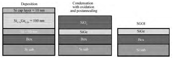
Fig. 1.
A schematic of the condensation process to manufacture SGOI.
SEMICONDUCTOR PHYSICS
B. Hamawandi1, M. Noroozi1, G. Jayakumar2, A. Ergül1, 3, K. Zahmatkesh1, M. S. Toprak1 and H. H. Radamson2
Abstract: In this study, the electrical properties of SiGe nanowires in terms of process and fabrication integrity, measurement reliability, width scaling, and doping levels were investigated. Nanowires were fabricated on SiGe-on oxide (SGOI) wafers with thickness of 52 nm and Ge content of 47%. The first group of SiGe wires was initially formed by using conventional I-line lithography and then their size was longitudinally reduced by cutting with a focused ion beam (FIB) to any desired nanometer range down to 60 nm. The other nanowire group was manufactured directly to a chosen nanometer level by using sidewall transfer lithography (STL). It has been shown that the FIB fabrication process allows manipulation of the line width and doping level of nanowires using Ga atoms. The resistance of wires thinned by FIB was 10 times lower than STL wires which shows the possible dependency of electrical behavior on fabrication method.
Key words: SiGe, FIB, STL, pattern transfer lithography, nanowires
| [1] |
?Noroozi M, Hamawandi B, Toprak M S, et al. Fabrication and thermoelectric characterization of GeSn nanowires. IEEE ULIS 2014 15th Int Conf Ultim Integr Silicon, 2014: 125 http://cn.bing.com/academic/profile?id=2052429245&encoded=0&v=paper_preview&mkt=zh-cn
|
| [2] |
Boukai A I, Bunimovich Y, Tahir-Kheli J, et al. Silicon nanowires as efficient thermoelectric materials. Nature, 2008, 451: 168 doi: 10.1038/nature06458
|
| [3] |
Jayakumar G, Garidis K, Hellstrom P E, et al. Fabrication and characterization of silicon nanowires using STL for biosensing applications. IEEE 2014 15th Int Conf Ultim Integr Silicon, 2014: 109 http://cn.bing.com/academic/profile?id=2152858635&encoded=0&v=paper_preview&mkt=zh-cn
|
| [4] |
Noroozi M, Ergul A, Abedin A, et al. Fabrications of size-controlled SiGe nanowires using I-line lithography and focused ion beam technique. ECS Trans, 2014, 64: 167 http://cn.bing.com/academic/profile?id=2004258090&encoded=0&v=paper_preview&mkt=zh-cn
|
| [5] |
Martinez J A, Provencio P P, Picraux S T, et al. Enhanced thermoelectric figure of merit in SiGe alloy nanowires by boundary and hole-phonon scattering. J Appl Phys, 2011, 110: 074317 doi: 10.1063/1.3647575
|
| [6] |
Halstedt J, Hellstro P E, Zhang Z, et al. A robust spacer gate process for deca-nanometer high-frequency MOSFETs. Microelectron Eng, 2006, 83: 434 doi: 10.1016/j.mee.2005.11.008
|
| [7] |
Burchhart T, Zeiner C, Lugstein A, et al. Tuning the electrical performance of Ge nanowire MOSFETs by focused ion beam implantation. Nanotechnology, 2011, 22: 035201 doi: 10.1088/0957-4484/22/3/035201
|
| [8] |
Gnaser H, Brodyanski A, Reuscher B. Focused ion beam implantation of Ga in Si and Ge: fluence-dependent retention and surface morphology. Surf Interface Anal, 2008, 40: 1415 doi: 10.1002/sia.v40:11
|
| [9] |
H?llstedt J, Hellstr?m P E, Radamson H H. Sidewall transfer lithography for reliable fabrication of nanowires and deca-nanometer MOSFETs. Thin Solid Films, 2008, 517: 117 doi: 10.1016/j.tsf.2008.08.134
|
| [10] |
Jayakumar G, Asadollahi A, Hellstr?m P E, et al. Silicon nanowires integrated with CMOS circuits for biosensing application. Solid State Electron, 2014, 98: 26 doi: 10.1016/j.sse.2014.04.005
|
| [11] |
Kole?nik-Gray M M, Lutz T, Collins G, et al. Contact resistivity and suppression of Fermi level pinning in side-contacted germanium nanowires. Appl Phys Lett, 2013, 103: 2013 http://cn.bing.com/academic/profile?id=1977154259&encoded=0&v=paper_preview&mkt=zh-cn
|
| [12] |
Wu X, Kulkarni J S, Collins G, et al. Synthesis and electrical and mechanical properties of silicon and germanium nanowires. Chem Mater, 2008, 20: 5954 doi: 10.1021/cm801104s
|
| [13] |
Bergin S M, Chen Y H, Rathmell A R, et al. The effect of nanowire length and diameter on the properties of transparent, conducting nanowire films. Nanoscale, 2012, 4: 1996 doi: 10.1039/c2nr30126a
|
| [14] |
Nur O, Willander M, Radamson H H, et al. Strain characterization of CoSi2/n-Si0.9Ge0.1/p-Si heterostructures. Appl Phys Lett, 1994, 64: 440 doi: 10.1063/1.111122
|
| [15] |
Ha?llstedt J, Blomqvist M, Persson P O, et al. The effect of carbon and germanium on phase transformation of nickel on Si1-x-yGexCy epitaxial layers. J Appl Phys, 2004, 95: 2397 doi: 10.1063/1.1645996
|
| [16] |
Bearden J A. X-ray wavelengths. Rev Mod Phys, 1967, 39: 78 doi: 10.1103/RevModPhys.39.78
|
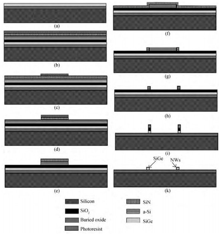
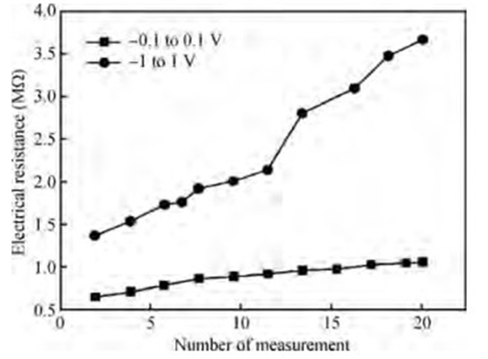
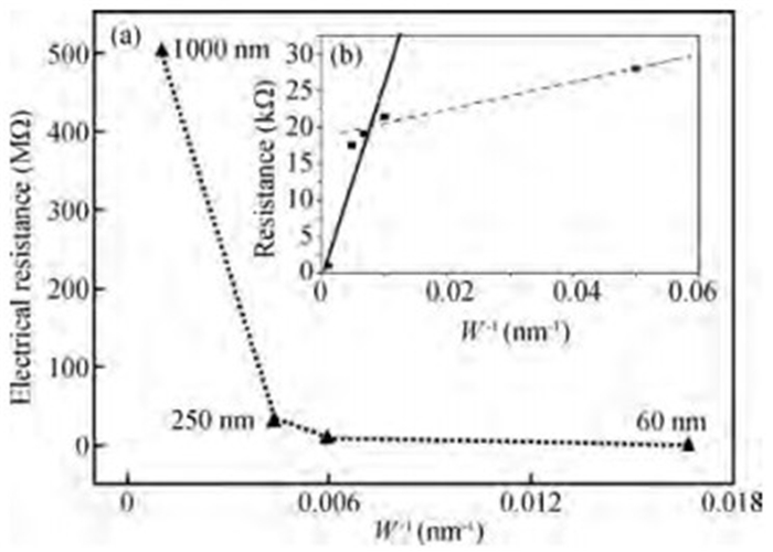
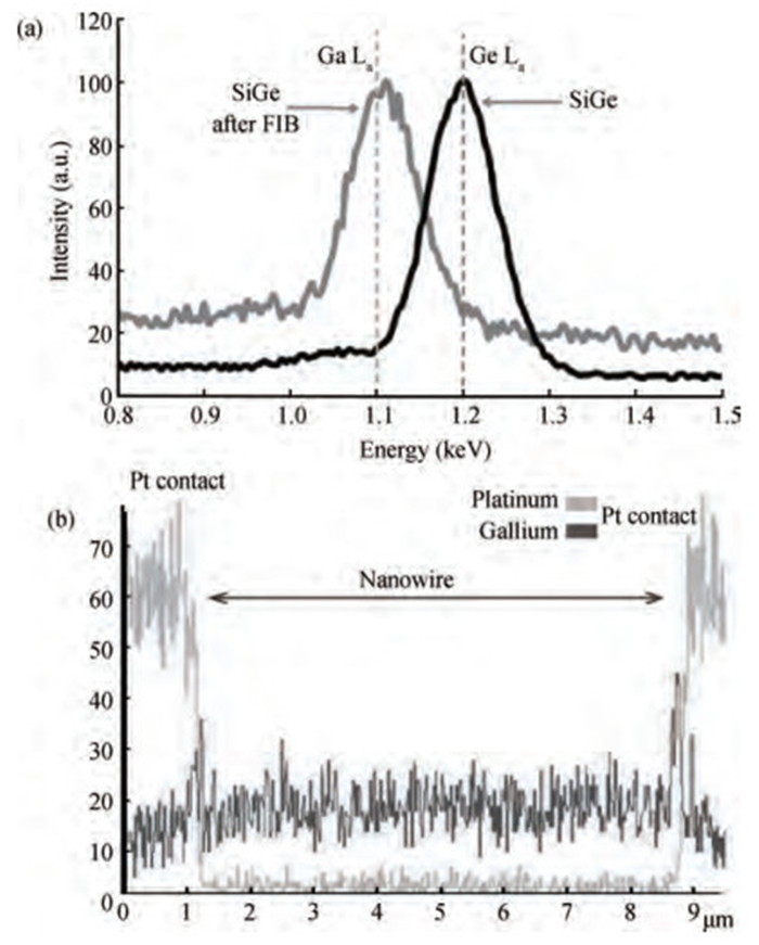
Table 1. Comparison of the resistance value for the 60 nm wide SiGe NWs fabricated by STL and FIB methods.

|
| [1] |
?Noroozi M, Hamawandi B, Toprak M S, et al. Fabrication and thermoelectric characterization of GeSn nanowires. IEEE ULIS 2014 15th Int Conf Ultim Integr Silicon, 2014: 125 http://cn.bing.com/academic/profile?id=2052429245&encoded=0&v=paper_preview&mkt=zh-cn
|
| [2] |
Boukai A I, Bunimovich Y, Tahir-Kheli J, et al. Silicon nanowires as efficient thermoelectric materials. Nature, 2008, 451: 168 doi: 10.1038/nature06458
|
| [3] |
Jayakumar G, Garidis K, Hellstrom P E, et al. Fabrication and characterization of silicon nanowires using STL for biosensing applications. IEEE 2014 15th Int Conf Ultim Integr Silicon, 2014: 109 http://cn.bing.com/academic/profile?id=2152858635&encoded=0&v=paper_preview&mkt=zh-cn
|
| [4] |
Noroozi M, Ergul A, Abedin A, et al. Fabrications of size-controlled SiGe nanowires using I-line lithography and focused ion beam technique. ECS Trans, 2014, 64: 167 http://cn.bing.com/academic/profile?id=2004258090&encoded=0&v=paper_preview&mkt=zh-cn
|
| [5] |
Martinez J A, Provencio P P, Picraux S T, et al. Enhanced thermoelectric figure of merit in SiGe alloy nanowires by boundary and hole-phonon scattering. J Appl Phys, 2011, 110: 074317 doi: 10.1063/1.3647575
|
| [6] |
Halstedt J, Hellstro P E, Zhang Z, et al. A robust spacer gate process for deca-nanometer high-frequency MOSFETs. Microelectron Eng, 2006, 83: 434 doi: 10.1016/j.mee.2005.11.008
|
| [7] |
Burchhart T, Zeiner C, Lugstein A, et al. Tuning the electrical performance of Ge nanowire MOSFETs by focused ion beam implantation. Nanotechnology, 2011, 22: 035201 doi: 10.1088/0957-4484/22/3/035201
|
| [8] |
Gnaser H, Brodyanski A, Reuscher B. Focused ion beam implantation of Ga in Si and Ge: fluence-dependent retention and surface morphology. Surf Interface Anal, 2008, 40: 1415 doi: 10.1002/sia.v40:11
|
| [9] |
H?llstedt J, Hellstr?m P E, Radamson H H. Sidewall transfer lithography for reliable fabrication of nanowires and deca-nanometer MOSFETs. Thin Solid Films, 2008, 517: 117 doi: 10.1016/j.tsf.2008.08.134
|
| [10] |
Jayakumar G, Asadollahi A, Hellstr?m P E, et al. Silicon nanowires integrated with CMOS circuits for biosensing application. Solid State Electron, 2014, 98: 26 doi: 10.1016/j.sse.2014.04.005
|
| [11] |
Kole?nik-Gray M M, Lutz T, Collins G, et al. Contact resistivity and suppression of Fermi level pinning in side-contacted germanium nanowires. Appl Phys Lett, 2013, 103: 2013 http://cn.bing.com/academic/profile?id=1977154259&encoded=0&v=paper_preview&mkt=zh-cn
|
| [12] |
Wu X, Kulkarni J S, Collins G, et al. Synthesis and electrical and mechanical properties of silicon and germanium nanowires. Chem Mater, 2008, 20: 5954 doi: 10.1021/cm801104s
|
| [13] |
Bergin S M, Chen Y H, Rathmell A R, et al. The effect of nanowire length and diameter on the properties of transparent, conducting nanowire films. Nanoscale, 2012, 4: 1996 doi: 10.1039/c2nr30126a
|
| [14] |
Nur O, Willander M, Radamson H H, et al. Strain characterization of CoSi2/n-Si0.9Ge0.1/p-Si heterostructures. Appl Phys Lett, 1994, 64: 440 doi: 10.1063/1.111122
|
| [15] |
Ha?llstedt J, Blomqvist M, Persson P O, et al. The effect of carbon and germanium on phase transformation of nickel on Si1-x-yGexCy epitaxial layers. J Appl Phys, 2004, 95: 2397 doi: 10.1063/1.1645996
|
| [16] |
Bearden J A. X-ray wavelengths. Rev Mod Phys, 1967, 39: 78 doi: 10.1103/RevModPhys.39.78
|


Article views: 3596 Times PDF downloads: 19 Times Cited by: 0 Times
Received: 16 February 2016 Revised: 11 May 2016 Online: Published: 01 October 2016
| Citation: |
B. Hamawandi, M. Noroozi, G. Jayakumar, A. Ergül, K. Zahmatkesh, M. S. Toprak, H. H. Radamson. Electrical properties of sub-100 nm SiGe nanowires[J]. Journal of Semiconductors, 2016, 37(10): 102001. doi: 10.1088/1674-4926/37/10/102001
****
B. Hamawandi, M. Noroozi, G. Jayakumar, A. Ergül, K. Zahmatkesh, M. S. Toprak, H. H. Radamson. Electrical properties of sub-100 nm SiGe nanowires[J]. J. Semicond., 2016, 37(10): 102001. doi: 10.1088/1674-4926/37/10/102001.

|
Swedish Foundation for Strategic Research “SSF” EM-011-0002
Scientific and Technological Research Council of Turkey TüB?TAK
Project support by the Swedish Foundation for Strategic Research “SSF” (No. EM-011-0002) and the Scientific and Technological Research Council of Turkey (No. TüB?TAK).
| [1] |
?Noroozi M, Hamawandi B, Toprak M S, et al. Fabrication and thermoelectric characterization of GeSn nanowires. IEEE ULIS 2014 15th Int Conf Ultim Integr Silicon, 2014: 125 http://cn.bing.com/academic/profile?id=2052429245&encoded=0&v=paper_preview&mkt=zh-cn
|
| [2] |
Boukai A I, Bunimovich Y, Tahir-Kheli J, et al. Silicon nanowires as efficient thermoelectric materials. Nature, 2008, 451: 168 doi: 10.1038/nature06458
|
| [3] |
Jayakumar G, Garidis K, Hellstrom P E, et al. Fabrication and characterization of silicon nanowires using STL for biosensing applications. IEEE 2014 15th Int Conf Ultim Integr Silicon, 2014: 109 http://cn.bing.com/academic/profile?id=2152858635&encoded=0&v=paper_preview&mkt=zh-cn
|
| [4] |
Noroozi M, Ergul A, Abedin A, et al. Fabrications of size-controlled SiGe nanowires using I-line lithography and focused ion beam technique. ECS Trans, 2014, 64: 167 http://cn.bing.com/academic/profile?id=2004258090&encoded=0&v=paper_preview&mkt=zh-cn
|
| [5] |
Martinez J A, Provencio P P, Picraux S T, et al. Enhanced thermoelectric figure of merit in SiGe alloy nanowires by boundary and hole-phonon scattering. J Appl Phys, 2011, 110: 074317 doi: 10.1063/1.3647575
|
| [6] |
Halstedt J, Hellstro P E, Zhang Z, et al. A robust spacer gate process for deca-nanometer high-frequency MOSFETs. Microelectron Eng, 2006, 83: 434 doi: 10.1016/j.mee.2005.11.008
|
| [7] |
Burchhart T, Zeiner C, Lugstein A, et al. Tuning the electrical performance of Ge nanowire MOSFETs by focused ion beam implantation. Nanotechnology, 2011, 22: 035201 doi: 10.1088/0957-4484/22/3/035201
|
| [8] |
Gnaser H, Brodyanski A, Reuscher B. Focused ion beam implantation of Ga in Si and Ge: fluence-dependent retention and surface morphology. Surf Interface Anal, 2008, 40: 1415 doi: 10.1002/sia.v40:11
|
| [9] |
H?llstedt J, Hellstr?m P E, Radamson H H. Sidewall transfer lithography for reliable fabrication of nanowires and deca-nanometer MOSFETs. Thin Solid Films, 2008, 517: 117 doi: 10.1016/j.tsf.2008.08.134
|
| [10] |
Jayakumar G, Asadollahi A, Hellstr?m P E, et al. Silicon nanowires integrated with CMOS circuits for biosensing application. Solid State Electron, 2014, 98: 26 doi: 10.1016/j.sse.2014.04.005
|
| [11] |
Kole?nik-Gray M M, Lutz T, Collins G, et al. Contact resistivity and suppression of Fermi level pinning in side-contacted germanium nanowires. Appl Phys Lett, 2013, 103: 2013 http://cn.bing.com/academic/profile?id=1977154259&encoded=0&v=paper_preview&mkt=zh-cn
|
| [12] |
Wu X, Kulkarni J S, Collins G, et al. Synthesis and electrical and mechanical properties of silicon and germanium nanowires. Chem Mater, 2008, 20: 5954 doi: 10.1021/cm801104s
|
| [13] |
Bergin S M, Chen Y H, Rathmell A R, et al. The effect of nanowire length and diameter on the properties of transparent, conducting nanowire films. Nanoscale, 2012, 4: 1996 doi: 10.1039/c2nr30126a
|
| [14] |
Nur O, Willander M, Radamson H H, et al. Strain characterization of CoSi2/n-Si0.9Ge0.1/p-Si heterostructures. Appl Phys Lett, 1994, 64: 440 doi: 10.1063/1.111122
|
| [15] |
Ha?llstedt J, Blomqvist M, Persson P O, et al. The effect of carbon and germanium on phase transformation of nickel on Si1-x-yGexCy epitaxial layers. J Appl Phys, 2004, 95: 2397 doi: 10.1063/1.1645996
|
| [16] |
Bearden J A. X-ray wavelengths. Rev Mod Phys, 1967, 39: 78 doi: 10.1103/RevModPhys.39.78
|

 WeChat ID
Journal of Semiconductors © 2017 All Rights Reserved 京ICP備05085259號-2
 DownLoad: