


Fig. 1.
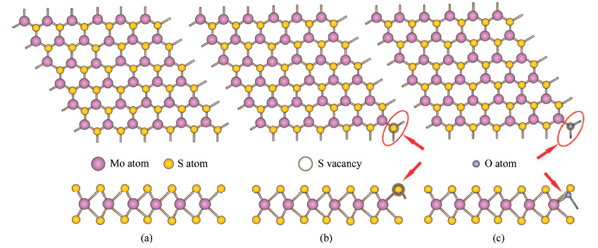
(Color online) Top and side view of layered MoS$_{2}$. (a) Undoped. (b) With S vacancy. (c) O-doped.
SEMICONDUCTOR PHYSICS
Anna V. Krivosheeva1, Victor L. Shaposhnikov1, Victor E. Borisenko1, Jean-Louis Lazzari2, Chow Waileong3, 4, Julia Gusakova1, 3 and Beng Kang Tay3, 4
Corresponding author: Anna V. Krivosheeva, Email: anna@nano.bsuir.edu.by
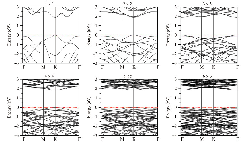
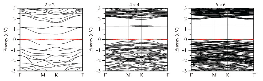
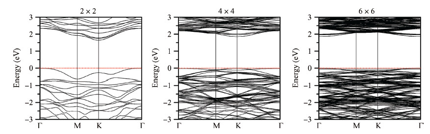
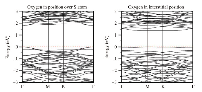
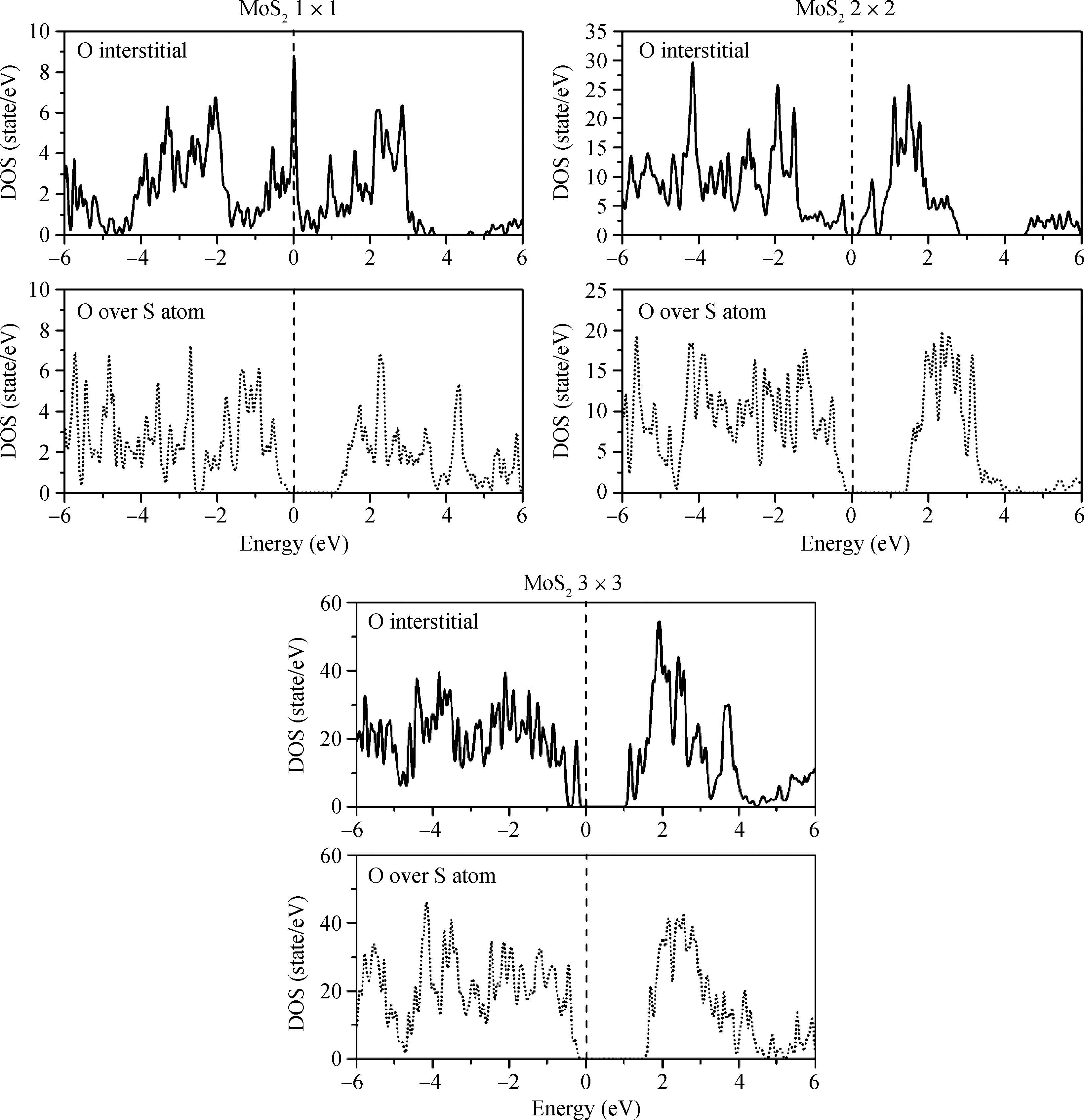
Abstract: Our theoretical findings demonstrate for the first time a possibility of band-gap engineering of monolayer MoS2 crystals by oxygen and the presence of vacancies. Oxygen atoms are revealed to substitute sulfur ones, forming stable MoS2-xOx ternary compounds, or adsorb on top of the sulfur atoms. The substituting oxygen provides a decrease of the band gap from 1.86 to 1.64 eV and transforms the material from a direct-gap to an indirect-gap semiconductor. The surface adsorbed oxygen atoms decrease the band gap up to 0.98 eV depending on their location tending to the metallic character of the electron energy bands at a high concentration of the adsorbed atoms. Oxygen plasma processing is proposed as an effective technology for such band-gap modifications.
Key words: two-dimensional crystal, molybdenum disulfide, band gap, vacancy, oxygen
| [1] | |
| [2] | |
| [3] | |
| [4] | |
| [5] | |
| [6] | |
| [7] | |
| [8] | |
| [9] | |
| [10] | |
| [11] | |
| [12] | |
| [13] | |
| [14] | |
| [15] | |
| [16] | |
| [17] | |
| [18] | |
| [19] | |
| [20] | |
| [21] | |
| [22] | |
| [23] | |
| [24] | |
| [25] | |
| [26] | |
| [27] | |
| [28] | |
| [29] | |
| [30] | |
| [31] |


Article views: 4827 Times PDF downloads: 86 Times Cited by: 0 Times
Received: 01 April 2015 Revised: Online: Published: 01 December 2015
| Citation: |
Anna V. Krivosheeva, Victor L. Shaposhnikov, Victor E. Borisenko, Jean-Louis Lazzari, Chow Waileong, Julia Gusakova, Beng Kang Tay. Theoretical study of defect impact on two-dimensional MoS2[J]. Journal of Semiconductors, 2015, 36(12): 122002. doi: 10.1088/1674-4926/36/12/122002
****
A. V. Krivosheeva, V. L. Shaposhnikov, V. E. Borisenko, J L. Lazzari, C Waileong, J Gusakova, B. K Tay. Theoretical study of defect impact on two-dimensional MoS2[J]. J. Semicond., 2015, 36(12): 122002. doi: 10.1088/1674-4926/36/12/122002.

|
| [1] | |
| [2] | |
| [3] | |
| [4] | |
| [5] | |
| [6] | |
| [7] | |
| [8] | |
| [9] | |
| [10] | |
| [11] | |
| [12] | |
| [13] | |
| [14] | |
| [15] | |
| [16] | |
| [17] | |
| [18] | |
| [19] | |
| [20] | |
| [21] | |
| [22] | |
| [23] | |
| [24] | |
| [25] | |
| [26] | |
| [27] | |
| [28] | |
| [29] | |
| [30] | |
| [31] |

 WeChat ID
Journal of Semiconductors © 2017 All Rights Reserved 京ICP備05085259號-2
 DownLoad:

