


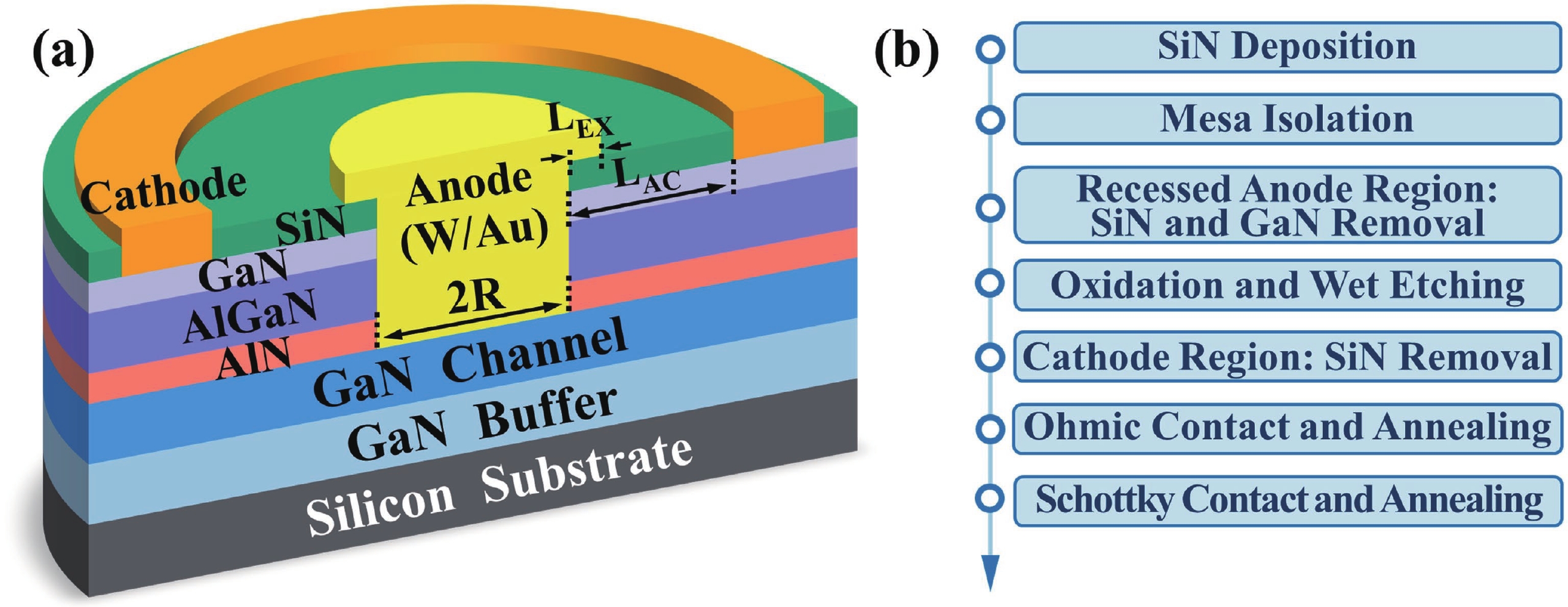
Fig. 1.
(Color online) (a) 3D cross-sectional structure and (b) process flow of the fabricated lateral AlGaN/GaN SBDs with self-terminated recessed anode.
ARTICLES
Jiahao Chen1, Tao Zhang1, , Ziqi Tao1, Kai Su1, Shengrui Xu1, Xiangdong Li2, Huake Su1, Yachao Zhang1, Yue Hao1 and Jincheng Zhang1,
Corresponding author: Tao Zhang, zhangtao@xidian.edu.cn; Jincheng Zhang, jchzhang@xidian.edu.cn
Abstract: In this letter, we demonstrate the effect of γ irradiation on the lateral AlGaN/GaN Schottky barrier diodes (SBDs) with self-terminated recessed anode structure and low work-function metal tungsten (W) as anode. For a comprehensive evaluation of the radiation-resistance performance of the device, the total dose of γ irradiation is up to 100 kGy with irradiation time of 20 h. Attributed to the barrier lowering effect of the W/GaN interface induced by γ irradiation observed in the experiment, the extracted turn-on voltage (VON) defined at anode forward current of 1 mA decreases from 0.47 to 0.43 V. Meanwhile, benefiting from the reinforced Schottky interface treated by post-anode-annealing, a high breakdown voltage (BV) of 1.75 kV is obtained for the γ-irradiated AlGaN/GaN SBD, which shows the promising application for the deep-space radiation environment and promotes the development of radiation-resistance research for GaN SBDs.
Key words: GaN, SBDs, γ irradiation, breakdown voltage, radiation-resistance
| [1] |
Wei X, Zhang X D, Tang W X, et al. 2.0 kV/2.1 mΩ·cm2 lateral p-GaN/AlGaN/GaN hybrid anode diodes with hydrogen plasma treatment. IEEE Electron Device Lett, 2022, 43(5), 693 doi: 10.1109/LED.2022.3159240
|
| [2] |
Liu X K, Wang H F, Wu J Y, et al. Vertical GaN Schottky barrier diode with record low contact resistivity on N-polarity using ultrathin ITO interfacial layer. IEEE Trans Electron Devices, 2023, 70(4), 1601 doi: 10.1109/TED.2023.3241565
|
| [3] |
Sun N, Wang R H, Huang H L, et al. 1500 V recessed-free GaN-based HEMTs with ultrathin barrier epitaxial structure. Appl Phys Lett, 2024, 125(23), 232102 doi: 10.1063/5.0235148
|
| [4] |
Zheng X, Feng S W, Peng C, et al. Evidence of GaN HEMT Schottky gate degradation after gamma irradiation. IEEE Trans Electron Devices, 2019, 66(9), 3784 doi: 10.1109/TED.2019.2928560
|
| [5] |
Liu S, Zhang J C, Zhao S L, et al. Characterization of trap states in AlN/GaN superlattice channel high electron mobility transistors under total-ionizing-dose with 60Co γ-irradiation. Appl Phys Lett, 2022, 120(20), 202102 doi: 10.1063/5.0088510
|
| [6] |
Zhang T, Zhang J C, Zhou H, et al. A > 3 kV/2.94 mΩ·cm2 and low leakage current with low turn-on voltage lateral GaN Schottky barrier diode on silicon substrate with anode engineering technique. IEEE Electron Device Lett, 2019, 40(10), 1583 doi: 10.1109/LED.2019.2933314
|
| [7] |
Zhang T, Wang Y, Zhang Y N, et al. Comprehensive annealing effects on AlGaN/GaN Schottky barrier diodes with different work-function metals. IEEE Trans Electron Devices, 2021, 68(6), 2661 doi: 10.1109/TED.2021.3074896
|
| [8] |
Gao J N, Jin Y F, Xie B, et al. Low ON-resistance GaN Schottky barrier diode with high VON uniformity using LPCVD Si3N4 compatible self-terminated, low damage anode recess technology. IEEE Electron Device Lett, 2018, 39(6), 859 doi: 10.1109/LED.2018.2830998
|
| [9] |
Lee J H, Im K S, Kim J K, et al. Performance of recessed anode AlGaN/GaN Schottky barrier diode passivated with high-temperature atomic layer-deposited Al2O3 layer. IEEE Trans Electron Devices, 2019, 66(1), 324 doi: 10.1109/TED.2018.2875356
|
| [10] |
Zhang T, Lv Y G, Li R H, et al. Current-collapse suppression of high-performance lateral AlGaN/GaN Schottky barrier diodes by a thick GaN cap layer. IEEE Electron Device Lett, 2021, 42(4), 477 doi: 10.1109/LED.2021.3057917
|
| [11] |
Xu R, Chen P, Liu M H, et al. 2.7-kV AlGaN/GaN Schottky barrier diode on silicon substrate with recessed-anode structure. Solid State Electron, 2021, 175, 107953 doi: 10.1016/j.sse.2020.107953
|
| [12] |
Wang H Y, Mao W, Yang C, et al. Lateral AlGaN/GaN Schottky barrier diode with arrayed p-GaN islands termination. IEEE Trans Electron Devices, 2021, 68(12), 6046 doi: 10.1109/TED.2021.3118326
|
| [13] |
Kang X W, Zheng Y K, Wu H, et al. Thin-barrier gated-edge termination AlGaN/GaN Schottky barrier diode with low reverse leakage and high turn-on uniformity. Semicond Sci Technol, 2021, 36(9), 094001 doi: 10.1088/1361-6641/ac0b93
|
| [14] |
Yang C Y, Wu J H, Chung C H, et al. Optimization of forward and reverse electrical characteristics of GaN-on-Si Schottky barrier diode through ladder-shaped hybrid anode engineering. IEEE Trans Electron Devices, 2022, 69(12), 6644 doi: 10.1109/TED.2022.3217999
|
| [15] |
Xu R, Chen P, Zhou J, et al. High power figure-of-merit, 10.6-kV AlGaN/GaN lateral Schottky barrier diode with single channel and sub-100-μm anode-to-cathode spacing. Small, 2022, 18(37), e2107301 doi: 10.1002/smll.202107301
|
| [16] |
Dai J X, Yu H M, Huang H L, et al. Recess-free thin-barrier AlGaN/GaN Schottky barrier diodes with ultra-low leakage current: Experiment and simulation study. Appl Phys Lett, 2024, 124(20), 202102 doi: 10.1063/5.0188134
|
| [17] |
Shi Y H, Li G X, He Y H, et al. Low turn-on voltage AlGaN/GaN Schottky barrier diode with a low work function anode and high work function field plate. Appl Phys Lett, 2024, 125(12), 123501 doi: 10.1063/5.0223396
|
| [18] |
Zhang T, Li R H, Lu J, et al. A 0.43 V/90 nA/mm lateral AlGaN/GaN Schottky barrier diode with plasma-free groove anode technique. IEEE Electron Device Lett, 2021, 42(12), 1747 doi: 10.1109/LED.2021.3123652
|
| [19] |
Visvkarma A K, Sehra K, Chanchal, et al. Impact of gamma radiations on static, pulsed I–V, and RF performance parameters of AlGaN/GaN HEMT. IEEE Trans Electron Devices, 2022, 69(5), 2299 doi: 10.1109/TED.2022.3161402
|
| [20] |
Aoshima K, Horita M, Jun S D. Correlation between non-ionizing energy loss and production rate of electron trap at EC–(0.12–0.20) eV formed in gallium nitride by various types of radiation. Appl Phys Lett, 2023, 122(1), 012106 doi: 10.1063/5.0128709
|
| [21] |
Tang Y, Zhou X T, Zhang B Y, et al. Comparison of proton irradiation effects on electrical properties of quasi-vertical and lateral GaN Schottky barrier diodes. IEEE Trans Nucl Sci, 2024, 72(1), 17 doi: 10.1109/TNS.2024.3520476
|
| [22] |
Pu T F, Li X B, Wu J Y, et al. Recessed anode AlGaN/GaN Schottky barrier diode for temperature sensor application. IEEE Trans Electron Devices, 2021, 68(10), 5162 doi: 10.1109/TED.2021.3105498
|
| [23] |
Liu J Y, He S, Xu G W, et al. The characteristics of line-shaped defects and their impact mechanism on device performance in β-Ga2O3 Schottky barrier diodes. Appl Phys Lett, 2025, 126(1), 012111 doi: 10.1063/5.0244107
|
| [24] |
Wu J Y, Liao Z L, Wang H F, et al. Ultra-low turn-on voltage (0.37 V) vertical GaN-on-GaN Schottky barrier diode via oxygen plasma treatment. Appl Phys Lett, 2023, 123(21), 213505 doi: 10.1063/5.0171406
|
| [25] |
Chen H Y, Zhang T, Su H K, et al. A 614 MW/cm2 AlGaN-channel Schottky barrier diode with high breakdown voltage and high temperature sensitivity. Appl Phys Lett, 2025, 126(1), 012112 doi: 10.1063/5.0248171
|
| [26] |
Roul B, Mukundan S, Chandan G, et al. Barrier height inhomogeneity in electrical transport characteristics of InGaN/GaN heterostructure interfaces. AIP Adv, 2015, 5(3), 037130 doi: 10.1063/1.4916264
|
| [27] |
Laurent M A, Gupta G, Suntrup D J III, et al. Barrier height inhomogeneity and its impact on (Al, In, Ga)N Schottky diodes. J Appl Phys, 2016, 119(6), 064501 doi: 10.1063/1.4941531
|
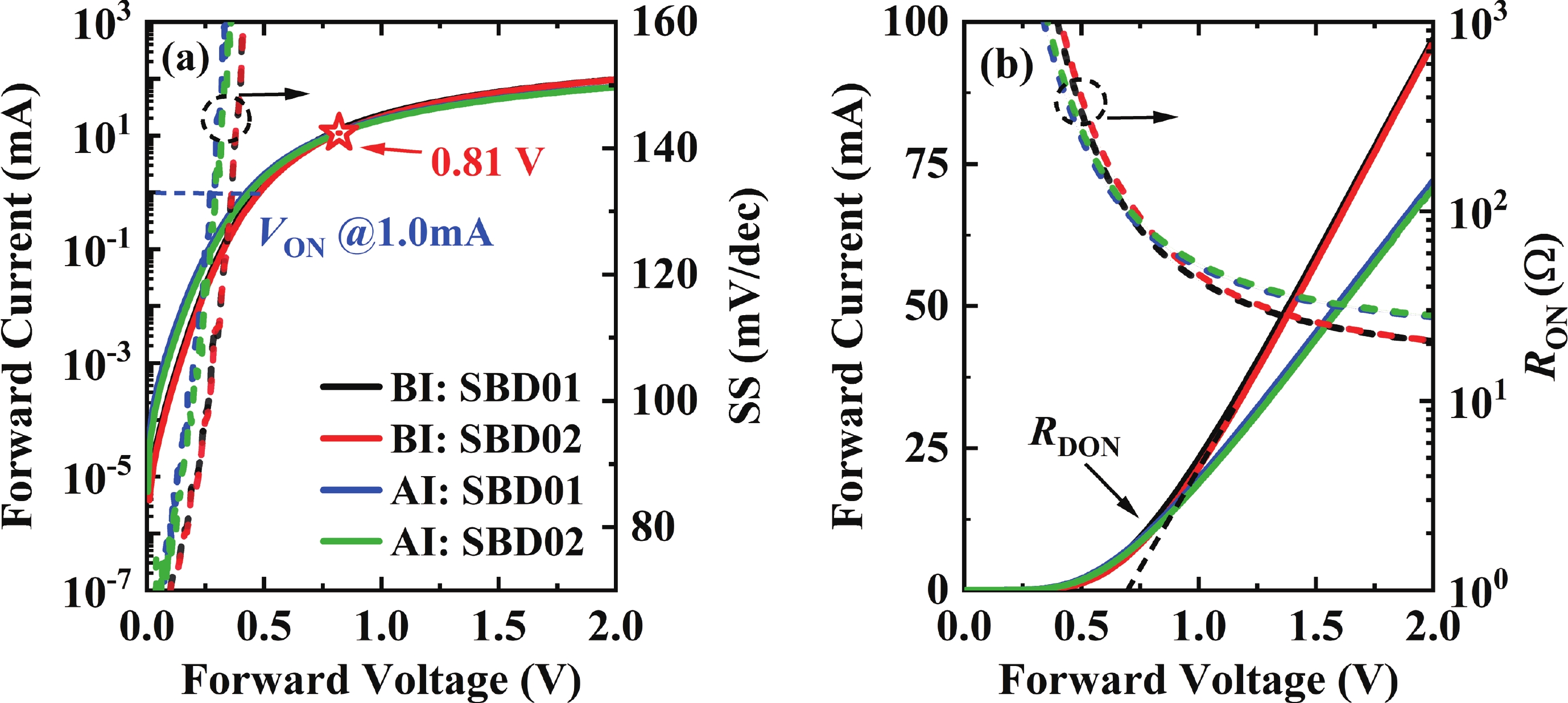
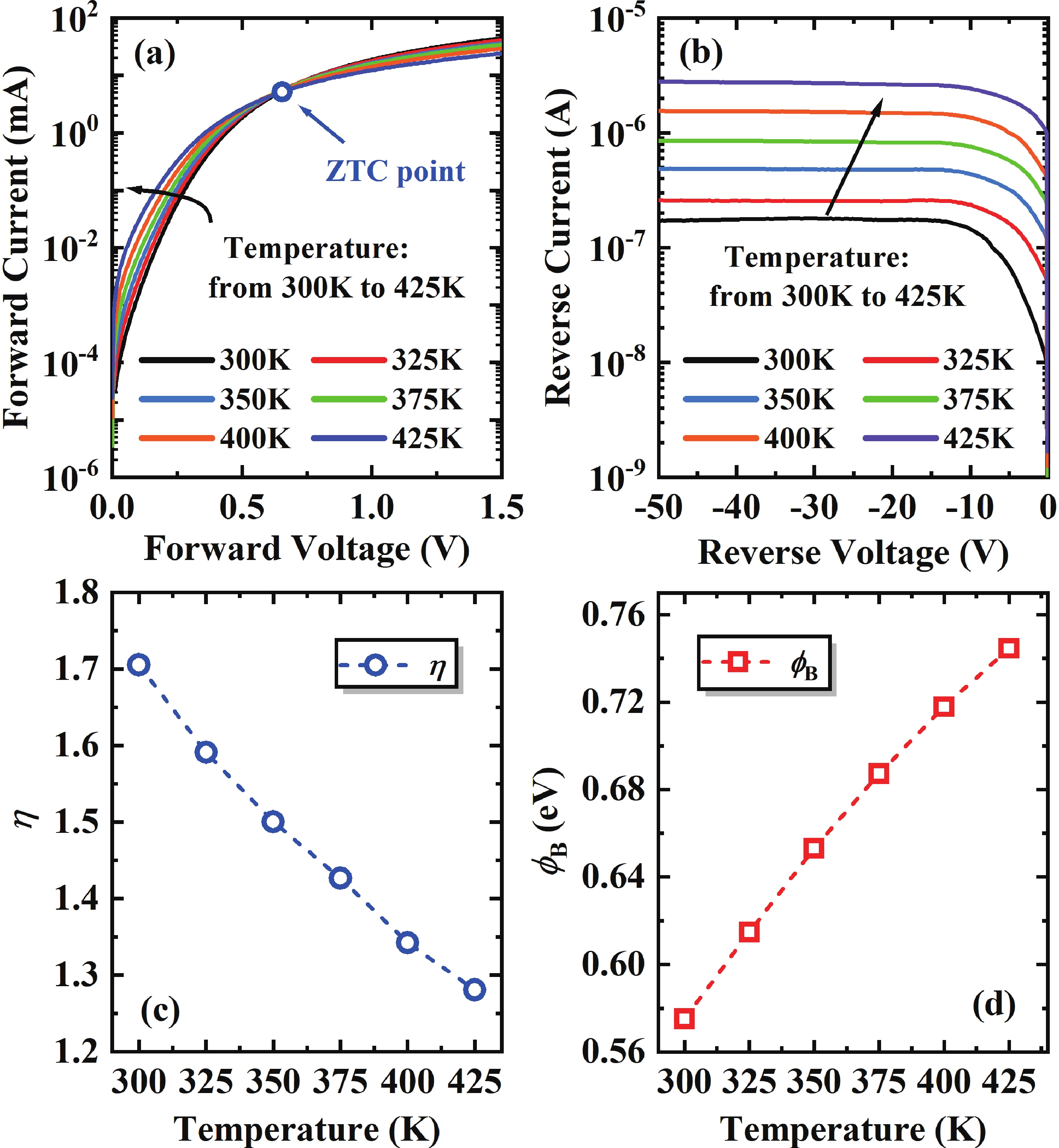
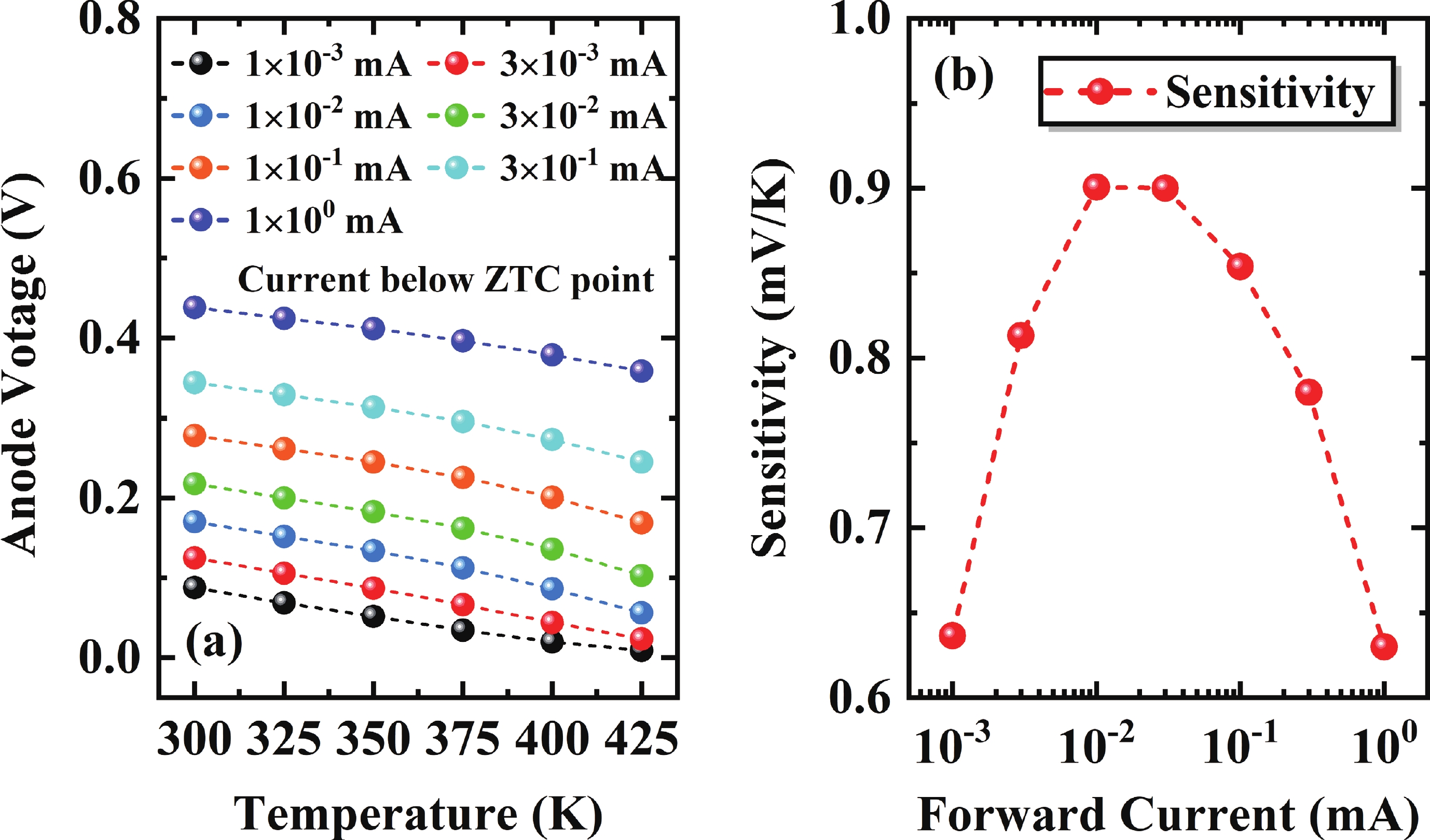
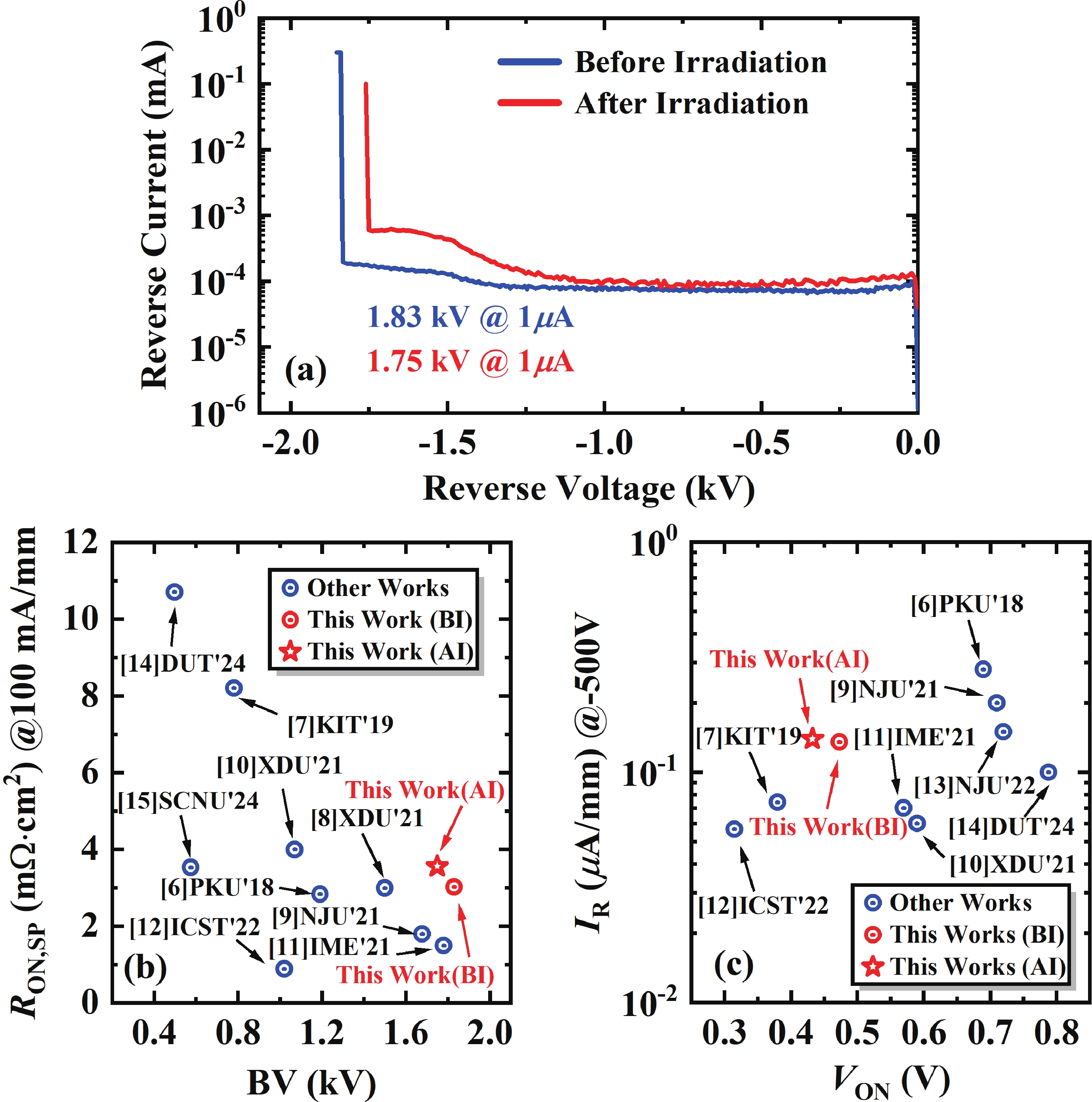
Table 1. VON, $\phi _{\mathrm{B}} $ and η of the fabricated AlGaN/GaN SBDs before and after γ irradiation.
| Parameter | Before irradiation | After irradiation | |||
| SBD 01 | SBD 02 | SBD 01 | SBD 02 | ||
| VON (V) | 0.466 | 0.480 | 0.426 | 0.439 | |
| $\phi _{\mathrm{B}} $ (eV) | 0.622 | 0.629 | 0.567 | 0.576 | |
| η | 1.480 | 1.466 | 1.711 | 1.702 | |
 DownLoad: CSV
| [1] |
Wei X, Zhang X D, Tang W X, et al. 2.0 kV/2.1 mΩ·cm2 lateral p-GaN/AlGaN/GaN hybrid anode diodes with hydrogen plasma treatment. IEEE Electron Device Lett, 2022, 43(5), 693 doi: 10.1109/LED.2022.3159240
|
| [2] |
Liu X K, Wang H F, Wu J Y, et al. Vertical GaN Schottky barrier diode with record low contact resistivity on N-polarity using ultrathin ITO interfacial layer. IEEE Trans Electron Devices, 2023, 70(4), 1601 doi: 10.1109/TED.2023.3241565
|
| [3] |
Sun N, Wang R H, Huang H L, et al. 1500 V recessed-free GaN-based HEMTs with ultrathin barrier epitaxial structure. Appl Phys Lett, 2024, 125(23), 232102 doi: 10.1063/5.0235148
|
| [4] |
Zheng X, Feng S W, Peng C, et al. Evidence of GaN HEMT Schottky gate degradation after gamma irradiation. IEEE Trans Electron Devices, 2019, 66(9), 3784 doi: 10.1109/TED.2019.2928560
|
| [5] |
Liu S, Zhang J C, Zhao S L, et al. Characterization of trap states in AlN/GaN superlattice channel high electron mobility transistors under total-ionizing-dose with 60Co γ-irradiation. Appl Phys Lett, 2022, 120(20), 202102 doi: 10.1063/5.0088510
|
| [6] |
Zhang T, Zhang J C, Zhou H, et al. A > 3 kV/2.94 mΩ·cm2 and low leakage current with low turn-on voltage lateral GaN Schottky barrier diode on silicon substrate with anode engineering technique. IEEE Electron Device Lett, 2019, 40(10), 1583 doi: 10.1109/LED.2019.2933314
|
| [7] |
Zhang T, Wang Y, Zhang Y N, et al. Comprehensive annealing effects on AlGaN/GaN Schottky barrier diodes with different work-function metals. IEEE Trans Electron Devices, 2021, 68(6), 2661 doi: 10.1109/TED.2021.3074896
|
| [8] |
Gao J N, Jin Y F, Xie B, et al. Low ON-resistance GaN Schottky barrier diode with high VON uniformity using LPCVD Si3N4 compatible self-terminated, low damage anode recess technology. IEEE Electron Device Lett, 2018, 39(6), 859 doi: 10.1109/LED.2018.2830998
|
| [9] |
Lee J H, Im K S, Kim J K, et al. Performance of recessed anode AlGaN/GaN Schottky barrier diode passivated with high-temperature atomic layer-deposited Al2O3 layer. IEEE Trans Electron Devices, 2019, 66(1), 324 doi: 10.1109/TED.2018.2875356
|
| [10] |
Zhang T, Lv Y G, Li R H, et al. Current-collapse suppression of high-performance lateral AlGaN/GaN Schottky barrier diodes by a thick GaN cap layer. IEEE Electron Device Lett, 2021, 42(4), 477 doi: 10.1109/LED.2021.3057917
|
| [11] |
Xu R, Chen P, Liu M H, et al. 2.7-kV AlGaN/GaN Schottky barrier diode on silicon substrate with recessed-anode structure. Solid State Electron, 2021, 175, 107953 doi: 10.1016/j.sse.2020.107953
|
| [12] |
Wang H Y, Mao W, Yang C, et al. Lateral AlGaN/GaN Schottky barrier diode with arrayed p-GaN islands termination. IEEE Trans Electron Devices, 2021, 68(12), 6046 doi: 10.1109/TED.2021.3118326
|
| [13] |
Kang X W, Zheng Y K, Wu H, et al. Thin-barrier gated-edge termination AlGaN/GaN Schottky barrier diode with low reverse leakage and high turn-on uniformity. Semicond Sci Technol, 2021, 36(9), 094001 doi: 10.1088/1361-6641/ac0b93
|
| [14] |
Yang C Y, Wu J H, Chung C H, et al. Optimization of forward and reverse electrical characteristics of GaN-on-Si Schottky barrier diode through ladder-shaped hybrid anode engineering. IEEE Trans Electron Devices, 2022, 69(12), 6644 doi: 10.1109/TED.2022.3217999
|
| [15] |
Xu R, Chen P, Zhou J, et al. High power figure-of-merit, 10.6-kV AlGaN/GaN lateral Schottky barrier diode with single channel and sub-100-μm anode-to-cathode spacing. Small, 2022, 18(37), e2107301 doi: 10.1002/smll.202107301
|
| [16] |
Dai J X, Yu H M, Huang H L, et al. Recess-free thin-barrier AlGaN/GaN Schottky barrier diodes with ultra-low leakage current: Experiment and simulation study. Appl Phys Lett, 2024, 124(20), 202102 doi: 10.1063/5.0188134
|
| [17] |
Shi Y H, Li G X, He Y H, et al. Low turn-on voltage AlGaN/GaN Schottky barrier diode with a low work function anode and high work function field plate. Appl Phys Lett, 2024, 125(12), 123501 doi: 10.1063/5.0223396
|
| [18] |
Zhang T, Li R H, Lu J, et al. A 0.43 V/90 nA/mm lateral AlGaN/GaN Schottky barrier diode with plasma-free groove anode technique. IEEE Electron Device Lett, 2021, 42(12), 1747 doi: 10.1109/LED.2021.3123652
|
| [19] |
Visvkarma A K, Sehra K, Chanchal, et al. Impact of gamma radiations on static, pulsed I–V, and RF performance parameters of AlGaN/GaN HEMT. IEEE Trans Electron Devices, 2022, 69(5), 2299 doi: 10.1109/TED.2022.3161402
|
| [20] |
Aoshima K, Horita M, Jun S D. Correlation between non-ionizing energy loss and production rate of electron trap at EC–(0.12–0.20) eV formed in gallium nitride by various types of radiation. Appl Phys Lett, 2023, 122(1), 012106 doi: 10.1063/5.0128709
|
| [21] |
Tang Y, Zhou X T, Zhang B Y, et al. Comparison of proton irradiation effects on electrical properties of quasi-vertical and lateral GaN Schottky barrier diodes. IEEE Trans Nucl Sci, 2024, 72(1), 17 doi: 10.1109/TNS.2024.3520476
|
| [22] |
Pu T F, Li X B, Wu J Y, et al. Recessed anode AlGaN/GaN Schottky barrier diode for temperature sensor application. IEEE Trans Electron Devices, 2021, 68(10), 5162 doi: 10.1109/TED.2021.3105498
|
| [23] |
Liu J Y, He S, Xu G W, et al. The characteristics of line-shaped defects and their impact mechanism on device performance in β-Ga2O3 Schottky barrier diodes. Appl Phys Lett, 2025, 126(1), 012111 doi: 10.1063/5.0244107
|
| [24] |
Wu J Y, Liao Z L, Wang H F, et al. Ultra-low turn-on voltage (0.37 V) vertical GaN-on-GaN Schottky barrier diode via oxygen plasma treatment. Appl Phys Lett, 2023, 123(21), 213505 doi: 10.1063/5.0171406
|
| [25] |
Chen H Y, Zhang T, Su H K, et al. A 614 MW/cm2 AlGaN-channel Schottky barrier diode with high breakdown voltage and high temperature sensitivity. Appl Phys Lett, 2025, 126(1), 012112 doi: 10.1063/5.0248171
|
| [26] |
Roul B, Mukundan S, Chandan G, et al. Barrier height inhomogeneity in electrical transport characteristics of InGaN/GaN heterostructure interfaces. AIP Adv, 2015, 5(3), 037130 doi: 10.1063/1.4916264
|
| [27] |
Laurent M A, Gupta G, Suntrup D J III, et al. Barrier height inhomogeneity and its impact on (Al, In, Ga)N Schottky diodes. J Appl Phys, 2016, 119(6), 064501 doi: 10.1063/1.4941531
|


Article views: 748 Times PDF downloads: 152 Times Cited by: 0 Times
Received: 23 April 2025 Revised: 09 July 2025 Online: Accepted Manuscript: 13 August 2025Uncorrected proof: 27 August 2025Published: 15 December 2025
| Citation: |
Jiahao Chen, Tao Zhang, Ziqi Tao, Kai Su, Shengrui Xu, Xiangdong Li, Huake Su, Yachao Zhang, Yue Hao, Jincheng Zhang. A γ-irradiated AlGaN/GaN Schottky barrier diode with barrier-decreased Schottky junction and high breakdown voltage[J]. Journal of Semiconductors, 2025, 46(12): 122501. doi: 10.1088/1674-4926/25040026
****
J H Chen, T Zhang, Z Q Tao, K Su, S R Xu, X D Li, H K Su, Y C Zhang, Y Hao, and J C Zhang, A γ-irradiated AlGaN/GaN Schottky barrier diode with barrier-decreased Schottky junction and high breakdown voltage[J]. J. Semicond., 2025, 46(12), 122501 doi: 10.1088/1674-4926/25040026

|
 Jiahao Chen received the B.Eng. degree from Fuzhou University in 2024. He is currently pursuing the Master degree with the School of Microelectronics, Xidian University. His research interest focuses on GaN-based electronic devices
 Tao Zhang received the Ph.D. degree from Xidian University in 2020. Currently, he is an associate professor at Xidian University. His research interest focuses on wide-bandgap semiconductor,as well as their applications in high-performance electronic and power devices
 Jincheng Zhang received the M.S. and Ph.D. degrees from Xidian University, Xi’an, China, in 2001 and 2004, respectively. He is currently a professor with Xidian University. His current research interests include wide-bandgap semiconductor GaN and diamond materials and devices
| [1] |
Wei X, Zhang X D, Tang W X, et al. 2.0 kV/2.1 mΩ·cm2 lateral p-GaN/AlGaN/GaN hybrid anode diodes with hydrogen plasma treatment. IEEE Electron Device Lett, 2022, 43(5), 693 doi: 10.1109/LED.2022.3159240
|
| [2] |
Liu X K, Wang H F, Wu J Y, et al. Vertical GaN Schottky barrier diode with record low contact resistivity on N-polarity using ultrathin ITO interfacial layer. IEEE Trans Electron Devices, 2023, 70(4), 1601 doi: 10.1109/TED.2023.3241565
|
| [3] |
Sun N, Wang R H, Huang H L, et al. 1500 V recessed-free GaN-based HEMTs with ultrathin barrier epitaxial structure. Appl Phys Lett, 2024, 125(23), 232102 doi: 10.1063/5.0235148
|
| [4] |
Zheng X, Feng S W, Peng C, et al. Evidence of GaN HEMT Schottky gate degradation after gamma irradiation. IEEE Trans Electron Devices, 2019, 66(9), 3784 doi: 10.1109/TED.2019.2928560
|
| [5] |
Liu S, Zhang J C, Zhao S L, et al. Characterization of trap states in AlN/GaN superlattice channel high electron mobility transistors under total-ionizing-dose with 60Co γ-irradiation. Appl Phys Lett, 2022, 120(20), 202102 doi: 10.1063/5.0088510
|
| [6] |
Zhang T, Zhang J C, Zhou H, et al. A > 3 kV/2.94 mΩ·cm2 and low leakage current with low turn-on voltage lateral GaN Schottky barrier diode on silicon substrate with anode engineering technique. IEEE Electron Device Lett, 2019, 40(10), 1583 doi: 10.1109/LED.2019.2933314
|
| [7] |
Zhang T, Wang Y, Zhang Y N, et al. Comprehensive annealing effects on AlGaN/GaN Schottky barrier diodes with different work-function metals. IEEE Trans Electron Devices, 2021, 68(6), 2661 doi: 10.1109/TED.2021.3074896
|
| [8] |
Gao J N, Jin Y F, Xie B, et al. Low ON-resistance GaN Schottky barrier diode with high VON uniformity using LPCVD Si3N4 compatible self-terminated, low damage anode recess technology. IEEE Electron Device Lett, 2018, 39(6), 859 doi: 10.1109/LED.2018.2830998
|
| [9] |
Lee J H, Im K S, Kim J K, et al. Performance of recessed anode AlGaN/GaN Schottky barrier diode passivated with high-temperature atomic layer-deposited Al2O3 layer. IEEE Trans Electron Devices, 2019, 66(1), 324 doi: 10.1109/TED.2018.2875356
|
| [10] |
Zhang T, Lv Y G, Li R H, et al. Current-collapse suppression of high-performance lateral AlGaN/GaN Schottky barrier diodes by a thick GaN cap layer. IEEE Electron Device Lett, 2021, 42(4), 477 doi: 10.1109/LED.2021.3057917
|
| [11] |
Xu R, Chen P, Liu M H, et al. 2.7-kV AlGaN/GaN Schottky barrier diode on silicon substrate with recessed-anode structure. Solid State Electron, 2021, 175, 107953 doi: 10.1016/j.sse.2020.107953
|
| [12] |
Wang H Y, Mao W, Yang C, et al. Lateral AlGaN/GaN Schottky barrier diode with arrayed p-GaN islands termination. IEEE Trans Electron Devices, 2021, 68(12), 6046 doi: 10.1109/TED.2021.3118326
|
| [13] |
Kang X W, Zheng Y K, Wu H, et al. Thin-barrier gated-edge termination AlGaN/GaN Schottky barrier diode with low reverse leakage and high turn-on uniformity. Semicond Sci Technol, 2021, 36(9), 094001 doi: 10.1088/1361-6641/ac0b93
|
| [14] |
Yang C Y, Wu J H, Chung C H, et al. Optimization of forward and reverse electrical characteristics of GaN-on-Si Schottky barrier diode through ladder-shaped hybrid anode engineering. IEEE Trans Electron Devices, 2022, 69(12), 6644 doi: 10.1109/TED.2022.3217999
|
| [15] |
Xu R, Chen P, Zhou J, et al. High power figure-of-merit, 10.6-kV AlGaN/GaN lateral Schottky barrier diode with single channel and sub-100-μm anode-to-cathode spacing. Small, 2022, 18(37), e2107301 doi: 10.1002/smll.202107301
|
| [16] |
Dai J X, Yu H M, Huang H L, et al. Recess-free thin-barrier AlGaN/GaN Schottky barrier diodes with ultra-low leakage current: Experiment and simulation study. Appl Phys Lett, 2024, 124(20), 202102 doi: 10.1063/5.0188134
|
| [17] |
Shi Y H, Li G X, He Y H, et al. Low turn-on voltage AlGaN/GaN Schottky barrier diode with a low work function anode and high work function field plate. Appl Phys Lett, 2024, 125(12), 123501 doi: 10.1063/5.0223396
|
| [18] |
Zhang T, Li R H, Lu J, et al. A 0.43 V/90 nA/mm lateral AlGaN/GaN Schottky barrier diode with plasma-free groove anode technique. IEEE Electron Device Lett, 2021, 42(12), 1747 doi: 10.1109/LED.2021.3123652
|
| [19] |
Visvkarma A K, Sehra K, Chanchal, et al. Impact of gamma radiations on static, pulsed I–V, and RF performance parameters of AlGaN/GaN HEMT. IEEE Trans Electron Devices, 2022, 69(5), 2299 doi: 10.1109/TED.2022.3161402
|
| [20] |
Aoshima K, Horita M, Jun S D. Correlation between non-ionizing energy loss and production rate of electron trap at EC–(0.12–0.20) eV formed in gallium nitride by various types of radiation. Appl Phys Lett, 2023, 122(1), 012106 doi: 10.1063/5.0128709
|
| [21] |
Tang Y, Zhou X T, Zhang B Y, et al. Comparison of proton irradiation effects on electrical properties of quasi-vertical and lateral GaN Schottky barrier diodes. IEEE Trans Nucl Sci, 2024, 72(1), 17 doi: 10.1109/TNS.2024.3520476
|
| [22] |
Pu T F, Li X B, Wu J Y, et al. Recessed anode AlGaN/GaN Schottky barrier diode for temperature sensor application. IEEE Trans Electron Devices, 2021, 68(10), 5162 doi: 10.1109/TED.2021.3105498
|
| [23] |
Liu J Y, He S, Xu G W, et al. The characteristics of line-shaped defects and their impact mechanism on device performance in β-Ga2O3 Schottky barrier diodes. Appl Phys Lett, 2025, 126(1), 012111 doi: 10.1063/5.0244107
|
| [24] |
Wu J Y, Liao Z L, Wang H F, et al. Ultra-low turn-on voltage (0.37 V) vertical GaN-on-GaN Schottky barrier diode via oxygen plasma treatment. Appl Phys Lett, 2023, 123(21), 213505 doi: 10.1063/5.0171406
|
| [25] |
Chen H Y, Zhang T, Su H K, et al. A 614 MW/cm2 AlGaN-channel Schottky barrier diode with high breakdown voltage and high temperature sensitivity. Appl Phys Lett, 2025, 126(1), 012112 doi: 10.1063/5.0248171
|
| [26] |
Roul B, Mukundan S, Chandan G, et al. Barrier height inhomogeneity in electrical transport characteristics of InGaN/GaN heterostructure interfaces. AIP Adv, 2015, 5(3), 037130 doi: 10.1063/1.4916264
|
| [27] |
Laurent M A, Gupta G, Suntrup D J III, et al. Barrier height inhomogeneity and its impact on (Al, In, Ga)N Schottky diodes. J Appl Phys, 2016, 119(6), 064501 doi: 10.1063/1.4941531
|

 WeChat ID
Journal of Semiconductors © 2017 All Rights Reserved 京ICP備05085259號(hào)-2

